
K-WANG
+086-15305925923
Service expert in industrial control field!


Product
Article
NameDescriptionContent
Adequate Inventory, Timely Service
pursuit of excellence


Ship control system
Equipment control system
Power monitoring system
Current position:
新闻动态
newS
Brand
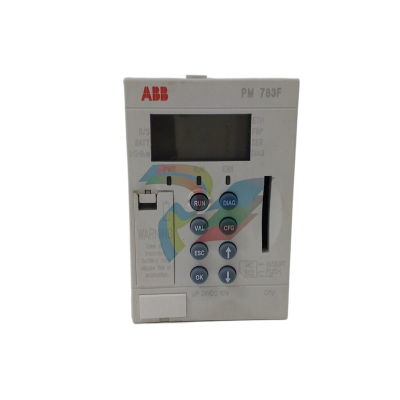
ABB D674A905U01 Sensor Display Control Unit
ABB D674A905U01 Sensor Display Control Unit
ABB D674A905U01 Sensor Display Control Unit
ENVIRONMENTAL SPECIFICATIONSThe maximum ambient temperature measured at the hottest point within the Triguard system
shall not be greater than 60 degrees centigrade.
Temperature operating: +5°C to +60°C
Temperature storage: -25°C to +70°C
Humidity 5% to 95% non-condensing at ambient <40°C
EMC/RFI Immunity Tested and certified to IEC 1131-Part 2 1994
Vibration/Shock Tested and certified to IEC 1131-Part 2 1994
Certification:
General Certification: Ref. SC300E Product Guide (ref 008-5209)
TRANSPORT AND HANDLING
The MSR04XI module must be transported and stored in its original packing material which
should be retained for this purpose.
TECHNICAL DESCRIPTION
PHYSICAL
The Serial Communications Module is a 9U high PCB with integral front panel and front and
rear connectors; a plug-in daughter board carries the RS232 interface circuits. Figure 1-1
shows the general layout, location of the connectors and front panel components.
Mechanical coding blocks
All Input/Output modules carry two mechanical coding blocks equipped with pins which mate
with holes in corresponding blocks in the chassis and prevent the module being inserted into
the wrong slot. The pins in the module blocks are factory installed in a pattern determined by
the module and corresponding set screws are removed from the chassis coding blocks to
enable fitting. Unused holes are plugged with set screws. The chassis mechanical coding
block configuration for this module is shown in Figure 2-1 .
Figure 2-1 Chassis mechanical coding block configurations
Links
The PCB has a total of nine links. For the top section of the PCB the links are located and
configured as follows:
Three LK1 links (3-pin) located approximately 80mm down from the top of the module, not user
configurable, link not fitted.
Three LK2 links (8-pin) located approximately 210mm down from the top of the module -
Module ID links which should always be fitted (refer to Figure 1-1).
On the lower section of the PCB are three further links, LK2, LK3 and LK4, located and
configured as follows:
LK2 (2-pin) located approximately 220mm down from the top of the module and 110mm in from
the front face, used in the voltage monitoring circuit, always fitted.
LK3 (3-pin) located beneath the plug in daughterboard. Used for 3-2-1-or 3-2-0 operation,
factory fitted hard wired, all pins linked for 3-2-1 mode.
LK4 (3-pin) located approximately 250mm down from the top of the module and 220mm from
the front face, used for the daughterboard clock speed setting, pins 1 and 2 linked.
Table 2-1. Default link settings
Link Default setting
LK1 (3 off x 3 pin) Links not fitted
LK2 (3 off x 8 pin) Fitted
LK2 (2 pin) Fitted
LK3 (3 pin) Hard wired (all pins linked)
LK4 (3 pin) Fitted (pins 1 & 2 linked)
EXTERNAL CONNECTIONS
Pinouts and signals for front panel connectors J4 to J6 through to J2 backplane are given in
Table 2-2.
Is your interface DTE (data terminal equipment) or DCE (data communications equipment)?:
The point of reference for all signals is the terminal (or PC).
Transmit and receive leads (2 or 3) can be reversed depending on the use of the equipment,
either DTE or DCE.
- YOKOGAWA
- Reliance
- ADVANCED
- SEW
- ProSoft
- WATLOW
- Kongsberg
- FANUC
- VSD
- DCS
- PLC
- man-machine
- Covid-19
- Energy and Gender
- Energy Access
- Renewable Integration
- Energy Subsidies
- Energy and Water
- Net zero emission
- Energy Security
- Critical Minerals
- A-B
- petroleum
- Mine scale
- Sewage treatment
- cement
- architecture
- Industrial information
- New energy
- Automobile market
- electricity
- Construction site
- HIMA
- ABB
- Rockwell
- Schneider Modicon
- Siemens
- xYCOM
- Yaskawa
- Woodward
- BOSCH Rexroth
- MOOG
- General Electric
- American NI
- Rolls-Royce
- CTI
- Honeywell
- EMERSON
- MAN
- GE
- TRICONEX
- Control Wave
- ALSTOM
- AMAT
- STUDER
- KONGSBERG
- MOTOROLA
- DANAHER MOTION
- Bentley
- Galil
- EATON
- MOLEX
- Triconex
- DEIF
- B&W
- ZYGO
- Aerotech
- DANFOSS
- KOLLMORGEN
- Beijer
- Endress+Hauser
- schneider
- Foxboro
- KB
- REXROTH
- YAMAHA
- Johnson
- Westinghouse
- WAGO
- TOSHIBA
- TEKTRONIX
- BENDER
- BMCM
- SMC
- HITACHI
- HIRSCHMANN
- XP POWER
- Baldor
- Meggitt
- SHINKAWA
- Other Brands
- UniOP
- KUKA
- IBA
- Beckhoff
- ADLINK
51
-
ADLINK HPCI-14S12U - Industrial Control Backplane 12PCI Backplane PCI-14S Passive Backplane
-
ADLINK PCIe-GIE74C - image acquisition card 4-CH GigE Vision PoE+ Frame Grabber
-
ADLINK PCI-8164 - control card 4-Axis Advanced Motion Controller Board
-
ADLINK PCIe-U304 - 4 Port USB3 PCIe Frame Grabbers USB Screw Hole Card
-
ADLINK PCI-9112 - Multi-Function Data Acquisition Card DAQ Card
-
ADLINK PCI-7432 - 51-12013-0A50 4-CH Isolated Numérique I/O PCI Cartes Digital I/O Card
-
ADLINK PCA-6106P3-0C1 REV.C1 - backplane 6-Slot Passive Backplane Board
-
ADLINK PCI-7224 - 24-CH Opto-Isolated Digital I/O PCI Board
-
ADLINK CPCI-7433R(G) - Digital Input Board Rear I/O CompactPCI Card
-
ADLINK EBP-13E4 - 51-46703-0A30 Industrial PC Backplane Passive Backplane
-
ADLINK PCIE-HDV62 - Image acquisition card High Definition Video Frame Grabber
-
ADLINK EBP-13E4 - 51-46703-0A30 Industrial Backplane Board Passive Backplane
-
ADLINK 90111-B1 / CPCI-6770 - PCB CPU MODULE CompactPCI Single Board Computer
-
ADLINK PCI-7248 - DATA ACQUISITION PCI CARD 48-CH Parallel Digital I/O Board
-
ADLINK PCI-7230 - 51-12003-0a50 board PCI7230 32-CH Isolated Digital I/O Card
-
ADLINK PCI2A000CB - 51-20000-0B30 Multi-Function DAQ Card Baseboard
-
ADLINK PCI-8134-005 - 4-Axis Motion Controller Card
-
ADLINK PCI-7224 - 24-CH Opto-Isolated Digital I/O PCI Card
-
ADLINK PCI-7434 - 64-CH Isolated Digital Output Card
-
ADLINK PCI-8132 - motion control card 2-Axis Servo & Stepper Controller
-
ADLINK PCI-8134 - Motion Controller PCI Card 4-Axis Controller Board
-
ADLINK PCI-8164 - Motion Control Card 51-12406-0A40 4-Axis Controller
-
ADLINK 51-12001-0C20 - Circuit Board Data Acquisition Interface Module Hardware
-
ADLINK NuPR0-840 - industrial control motherboard Full-Size PICMG CPU Board
-
ADLINK PCI-7444 - 51-12023-0A10 card 128-CH Isolated Digital Output Board
-
ADLINK PCI-1612B - data acquisition card 4-Port RS-232/422/485 Serial Communication Card
-
ADLINK PCI-6208V 009 - 8/16-CH 16-Bit Analog Output Cards PCB-I-E-482=6BX3
-
ADLINK NUPRO-935A/LV - industrial control motherboard Full-Size PICMG SBC Board
-
ADLINK PCI-9114DG - Multi-Function DAQ Card Data Acquisition PCI Card
-
ADLINK ACL-7130 - Data acquisition card Isolated Digital I/O Board
-
ADLINK ABX-6300D-4E1-BP - board ABX6300D4E1BP Video Interface Expansion Card
-
ADLINK CPCI-6940 - CPCI-6940/D1539/M16-0(EA)-000E 6U CompactPCI Processor Board
-
ADLINK NuPRO-760 - industrial control motherboard Half-Size PICMG SBC CPU Board
-
ADLINK IMB-M42H (G)-0020 - industrial control motherboard LGA1155 Micro-ATX Mainboard
-
ADLINK RTV-24 / PCI-MP4S - 51-12519-1C30 4-Channel Real Time Video Capture Board
-
ADLINK PCI-8134 - 4-Axis Servo & Stepper Motion Controller Card
-
ADLINK MXC-6101D - V.PC000.002.ST.00 Box PC Configurable Embedded Computer
-
ADLINK PCI-8134A - 51-12421-0A10 Motion Control Card 4-Axis Controller Card
-
ADLINK DIN-100S / DIN-100SA1 - Technology SCSI-II TB 100-PIN Terminal Block Board
-
ADLINK DIN-812M001 / DIN812M001 - 51-14034-0A1 51140340A1 Terminal Module Breakout Interface
-
ADLINK PCI-8164 - Servo motion control 4-Axis Advanced Controller Card
-
ADLINK PCIe-GIE64 - Acquisition card GigE Vision PoE+ Frame Grabber
-
ADLINK M-302 - Industrial control motherboard ATX PC Board Mainboard
-
ADLINK PCI-8134 - Motion Controller PCI Card 4-Axis Controller Board
-
ADLINK PCI-RTV24 - Image capture card Analog Video Frame Grabber
-
ADLINK PCI-8102 - Motion control card 2-Axis Servo & Stepper Controller Board
-
ADLINK PCI-9112 REV.B1 - Card Multi-Function Data Acquisition Card
-
ADLINK HSI-DI32-M-N / HSL-TB32-M-DIN - Discrete I/O MODULE Distributed Automation Module System
-
ADLINK PCI-7296 - IO card REV.A3 96-CH Parallel Digital I/O Card
-
ADLINK DIN-814P-A4 / 814Y - terminal board Motion Control Interface Block
-
ADLINK DIN-814P-A4 - 51-14056-0A10 PCB-I-E-2736=ZA01 Screw Terminal Board Breakout
-
ADLINK M-322 - motherboard Industrial Control Computer Mainboard
-
ADLINK NUPRO-406 REV:B1 - industrial control motherboard Full-Size PICMG CPU Board
-
ADLINK AMP-204C - card DSP-Based 4-Axis Advanced Pulse-Train Controller
-
ADLINK HPCI14S REV.B1 - industrial computer baseboard 14-Slot Passive Backplane
-
ADLINK PCI-7250 - 8-CH Relay Output & 8-CH Isolated DI PCI Card
-
ADLINK EBP-13E2 - baseplate Passive Backplane Industrial Computer Chassis Board
-
ADLINK LPCI-3488A - PCI-GPIB card 51-12801-0A30 acquisition card IEEE-488 Interface Board
-
ADLINK PCI-6216V-GL - 51-12201-0C30 16-CH 16-Bit Voltage Analog Output Card
-
ADLINK ACL-8454 - 16-CH Isolated Digital I/O & 4-CH Counter Card
-
ADLINK HPCI-9S7U - backplane Passive Backplane Compatible with NuPRO-A301 852 841 842
-
ADLINK DAQ-2010-007 - Simultaneous-Sampling Multi-Function Data Acquisition Card
-
ADLINK MP-C154 - 51-64205-0A10 Motion Control Card 4-Axis Controller Board
-
ADLINK MXE-202/mSSD16B/WiFi-BT - Matrix Rugged I/O Platform Embedded Fanless Computer
-
ADLINK CM-920-R-17 - PC/104-Plus Single Board Computer Module Intel Celeron M
-
ADLINK PCI-7250 NSMP - 8-CH Relay Output & 8-CH Isolated DI Card
-
ADLINK PCI-8164 - 4-Axis Motion Controller PCI Card W/ Cable and Breakout Box
-
ADLINK EMX-100 - Ethernet-based 4-axis Motion Controllers Distributed Motion Module
-
ADLINK PCI-8134A - Press control card 4-Axis Motion Controller Board
-
ADLINK M-845EG REV:3.2 - industrial motherboard Pentium 4 Socket 478 Micro-ATX
-
ADLINK PCI-9114A Rev A2 DG - card High-Resolution Multi-Function Data Acquisition Board
-
ADLINK IEC-915GV - REV 1.1 Industrial motherboard Socket 478 CPU Board
-
ADLINK PCI-9111DG(G) - Data Acquisition Card Multi-Function DAQ Card
-
ADLINK HPCI-15S10 REV:B2 - Industrial computer base plate Passive Backplane Board
-
ADLINK NuPR0-840 / NuPR0-840DV - industrial control motherboard Full-size PICMG CPU Board
-
ADLINK RTV-24 / PCI-MP4S - 51-12519-1C30 4-Channel Real Time Video Capture Board
-
ADLINK NUPRO-780 - industrial control motherboard Pentium III Single Board Computer
-
ADLINK PCI-7296 - 0050 card 96-CH Opto-Isolated Parallel DIO Card Set
-
ADLINK NUPRO-780 - industrial control motherboard PICMG Full-Size SBC
-
ADLINK PCI-7248 - 51-12006-0A3 002 Pci 7248 48-CH Parallel Digital I/O Card
-
ADLINK PCI-7230 - 32-CH Isolated Digital I/O Card
-
ADLINK AMP-204C - motion control card 4-Axis Advanced Controller Board
-
ADLINK PCI-1714UL - Card Ultra High-Speed 4-CH Simultaneous Sampling DAQ
-
ADLINK NuPRO-E330 - industrial computer equipment motherboard PICMG 1.3 SHB SBC
-
ADLINK AMP-204C - DSP-Based 4-Axis Advanced Pulse-Train Motion Controller Module
-
ADLINK PCI-7256 - 001 51-12206-0A2 REV.A2 LPCI-7256 16-CH Latching Relay Output Card
-
ADLINK ND6050 - NUDAM DIGITAL I/0 MODULE Distributed I/O Unit
-
ASEM BM100 - Box PC Embedded Fanless Industrial Computer
-
ADLINK PCI-7250 - PCI Acquisition Card 8-CH Relay Output & Isolated DI Board
-
ADLINK PCI-8164 - Servo motion control 4-Axis Controller Card
-
ADLINK NuPRO-A40H - Industrial Motherboard 51-41807-1A30 OSP LGA1155 H61
-
ADLINK ADMAX X300 SERVER - 51066010-0A30 motherboard Multi-Processor Mainboard
-
ADLINK CMe-GIE62+ - 51-32903-0A30 control card PC/104-Plus GigE Vision Frame Grabber
-
ADLINK NUPRO-780 - industrial control motherboard Full-Size PICMG SBC CPU Board
-
ADLINK ETX-AT-N270-18/GKTEL - 51-71111-OB10 motherboard ETX CPU Module Board
-
ADLINK DIN-812M - interface module Terminal Block Connection Board
-
ADLINK IMB-M42H - industrial control motherboard LGA1155 Micro-ATX Mainboard
-
ADLINK PXIS-2508 - 8-slot 3U PXI Instrument Chassis Power Hardware Assembly
-
ADLINK AMP-208C - Motion Control card DSP-Based 8-Axis Pulse-Train Controller
-
ADLINK PCI-9111 / PCI-9111DG - Multi-Function Data Acquisition Card DAQ Board
-
ADLINK IEEE-488 GPIB card - Bus Interface Controller Communication Board
-
ADLINK RTV-24 - 51-12519-1C30 image acquisition card Video Frame Grabber Card
-
ADLINK TB-24P/24-01 - Board 24 Way Screw Terminal Breakout Board
-
ADLINK HSL-DI16DO16-DB-NN - 51-23015-0A40 Distributed Discrete I/O Module Set
-
ADLINK PCI-7442 - switch quantity card data acquisition card 64-CH Isolated Card
-
ADLINK ACL-7130 REV. B2 - industrial control capture card Isolated Digital I/O PCI Card
-
ADLINK PCI-6S / PCI6S - Backplane 6-Slot Passive Backplane Chassis Board
-
ADLINK ACL-8113A - card Isolated Digital Input Card
-
ADLINK CPCI-6208V-003 - board cPCI CompactPCI 8-CH Analog Output Card
-
ADLINK DIN-100S-01(G) - SCSI 100-Pin Terminal Block Interface Board
-
ADLINK PCI-7433 - Isolated Digital Input Card 64-CH
-
ADLINK PCI-9812 - Synchronous sampling analog input card High-Speed DAQ Board
-
ADLINK PCI-7434 REV.B1 - PLOTECH PCB-I-E-1182=6EX2 64-CH Isolated Digital Output Card
-
ADLINK PCIe-RTV24 - 51-18016-0A20 4-CH Real-Time Video Capture Card PCIe Frame Grabber
-
ADLINK PCI-8144 / PCI-8144N - Motion control card 4-Axis Stepper Motor Controller
-
ADLINK DIN-68S-01 - terminal board 68-Pin Connector Terminal Block
-
ADLINK MP-C154 - Motion control card 4-Axis Advanced Controller Card
-
ADLINK PCI-7248 (G) - Motherboard 48-CH Parallel Digital I/O Card
-
ADLINK MXE-1301(G) - Intel Atom D2550+NM10 MXE 1300 Series 93-4130-0030 Embedded Computer
-
ADLINK PRO-841 Rev 2.0 / PRO-060907000670 - CPU 2.26GHz & RAM Industrial PC Board
-
ADLINK NuPRO-E330 - Industrial Motherboard System Host Board PICMG 1.3 SHB
-
ADLINK EBP-13E2 - Passive Backplane Industrial Chassis Baseboard
-
ADLINK PCI-8154 - 4-axis Motion Control Card Servo & Stepper Controller Board
-
ADLINK NuPrO-596 REV.B1 - industrial control motherboard Half-size PICMG CPU Board
-
ADLINK PCI-7852 / PCI-7851 - PLOTECH High-Speed Link Control Card Interface Board
-
ADLINK PCI-9112 - 51-12252-0D20 data acquisition card Multi-Function DAQ
-
ADLINK PCI-9112 - Circuit Board 51-12252-0C20 Multi-Function Data Acquisition Card
-
ADLINK NUPRO-761 REV:1.1 - industrial control motherboard PICMG Full-Size CPU Board

K-JIANG

Add: Jimei North Road, Jimei District, Xiamen, Fujian, China
Tell:+86-15305925923