
K-WANG


Microchip dsPIC30F series 16 bit high-performance digital signal controller
Microchip dsPIC30F High Performance 16 Bit Digital Signal Controller Field Application and Troubleshooting Guide
In the fields of industrial control, motor drive, power electronics, and automotive electronics, Microchip's dsPIC30F series digital signal controller (DSC) has become the core of many real-time control systems by perfectly integrating the control capabilities of a 16 bit microcontroller (MCU) with the computational performance of a digital signal processor (DSP). This series of devices provides processing power of up to 30 MIPS, with built-in up to 144KB FLASH, 8KB RAM, and 4KB EEPROM, and integrates rich peripherals such as PWM, QEI, CAN, multi-channel ADC, etc. It is widely used in three-phase AC motor control, switched reluctance motors, brushless DC motors, UPS power supplies, and sensor data acquisition scenarios.
However, as the product lifecycle evolves, engineers often face difficulties in firmware debugging, abnormal peripheral configurations, power issues, communication failures, and even the need for replacement after chip discontinuation. This article is based on the official technical manual of the dsPIC30F series. From the perspective of on-site maintenance and troubleshooting, it systematically outlines the architecture key points, common peripheral fault diagnosis methods, development tool usage skills, and upgrade migration strategies of this DSC, helping embedded engineers quickly locate problems and restore stable system operation.
Chapter 1: Core Architecture and Exception Handling of dsPIC30F
1.1 Architecture Overview
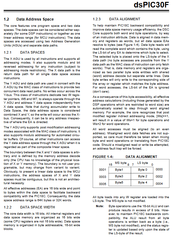
The dsPIC30F adopts an improved Harvard architecture with an instruction width of 24 bits and a data path of 16 bits. The program counter (PC) is 23 bits (with a minimum bit constant of 0) and has a linear addressing capability of 4M x 24 bit program memory. The data space is 64KB (32K words) and is divided into two data blocks, X and Y. DSP instructions can simultaneously take one operand from each of the X and Y spaces, while MCU instructions consider both as continuous linear spaces. This design not only ensures the convenience of traditional MCU programming, but also provides single cycle dual data reading capability for algorithms such as FFT and FIR filtering.
Key performance indicators:
Maximum 120MHz clock input (4 x/8 x/16 x PLL), 30 MIPS
16 × 16 bit working register array (W0~W15), W15 serves as the software stack pointer
Two 40 bit accumulators with optional saturation logic
40 level barrel shifter (single cycle left shift 16 positions or right shift 15 positions)
Single cycle 16 × 16 bit multiply accumulate (MAC)
Zero overhead loop support (DO/REPEAT instruction)
1.2 Common Exception and Trap Handling
The dsPIC30F has 15 exception sources (excluding reset), including 7 traps and 8 programmable priority interrupts. A trap is an unshieldable nested interrupt used to capture serious errors. The common traps and troubleshooting methods on site are as follows:
Address Error Trap
Trigger condition:
Unaligned word data access (e.g. reading 16 bit data from odd addresses)
Accessing unrealized data address space
Never implemented program address space indexing
Attempting to retrieve a pointer from the vector address space
On site diagnosis:
Check if there are any word operations on byte variables or address misalignment caused by pointer cast in the code.
Use MPLAB SIM emulator to enable 'Address Error Detection' and reproduce the fault.
If the trap occurs in the Interrupt Service Routine (ISR), check if the stack overflows (W15 exceeds the SPLIM setting).
Arithmetic Error Trap
Trigger scenario:
Zero division operation (the divisor in the DIV instruction is 0)
Accumulator overflow (overflow from bit 31 without using protection bit)
Catastrophic overflow (overflow from bit 39 and saturation disabled)
Exclusion method:
Check the divisor register before the division instruction, and if it is zero, jump to the processing code.
Enable accumulator saturation mode (SATA/SATB bits in CORCON register) to prevent erroneous results after overflow.
If precise overflow handling is not required, a reset instruction or null operation can be placed in the trap vector, but it is recommended to record the error status.
Stack Error Trap
Trigger condition: Stack pointer W15>SPLIM (overflow) or W15<0x0200 (underflow).
handle:
Set SPLIM to the highest stack address in the initialization code.
Check the depth of interrupt nesting to ensure that the stack size is sufficient.
If DSP instructions are used and a large number of fields are simultaneously loaded, the stack needs to be manually increased.
1.3 Hardware Reset and Power Monitoring
The dsPIC30F supports multiple reset sources: power on reset (POR), external MCLR reset, watchdog reset (WDT), programmable under voltage reset (PBOR), and RESET command. The most common reasons for inexplicable reset on site are undervoltage detection and watchdog timeout.
Under voltage reset (BOR): When VDD drops below the set threshold (e.g. 2.5V system drops to 2.3V), BOR will be forcibly reset. If the system power supply is unstable (such as voltage drop caused by the start of a large motor), the BOR can be disabled through the configuration word or a higher threshold BOR option can be used instead.
Watchdog Timer (WDT): default enabled (factory configuration word WDTEN=1). If the CLRWDT instruction is not executed in a timely manner in the main loop, a reset will be triggered after a few milliseconds. During the development phase, it is recommended to disable WDT in the configuration word or control it through the _SWDTEN software.
Reason identification for reset: Read the RCON register (reset control register), where bits such as BOR, WDTO, EXTR can indicate the last reset source. Saving this value during firmware startup and outputting it through the communication port greatly facilitates remote fault diagnosis.
Chapter 2 Troubleshooting of Advanced Analog Peripherals
2.1 10 bit/12 bit ADC module
The dsPIC30F offers two types of ADCs: a 500 ksps 10 bit ADC and a 100 ksps 12 bit ADC, both of which support up to 16 channels, differential input, and multi-channel sample and hold. Common ADC faults on site include conversion value jumping, excessive deviation, or complete non conversion.
Problem 1: The ADC conversion result always remains 0 or at full scale
Possible reasons:
The ADC module is not properly enabled (ADON bit is 0)
Insufficient sampling time (SAMC bit set too small, internal capacitor not charged to input voltage)
Reference voltage configuration error (VCFG bit selected non-existent pin)
Troubleshooting process:
Check ADCONx register: ADON=1, ADFM result alignment meets expectations.
Increase sampling time: for example, changing SAMC from 3TAD to 31TAD, or using automatic sampling triggering.
If using external Vref+and Vref - pins, ensure that the circuit board is connected to the correct voltage (not suspended).
Single step debugging: Write ADCON1bits. SAMP=1 to start sampling, delay, then set SAMP=0 to start conversion, and observe the DONE bit.
Problem 2: Nonlinear or noisy conversion results
Reason:
There is high-frequency digital signal (such as PWM, SPI clock) crosstalk near the analog input pins.
Internal Vref is unstable.
The ADC clock is higher than the recommended value (the maximum ADCLK of a 10 bit ADC is about 5MHz).
Solution:
Separate analog and digital ground on PCB and connect them at a single point.
Add RC low-pass filtering (R=1k Ω, C=0.1μF)。
Place the CPU in SLEEP or IDLE mode during conversion to reduce digital noise (ADC can operate in sleep mode).
Using oversampling and averaging techniques: taking the average after 8 consecutive conversions to effectively improve resolution.
2.2 Low Voltage Detection (LVD)
The LVD module allows software to set a voltage trigger point (internal reference voltage) that generates an interrupt (priority 7, non maskable) when VDD is below a threshold. This is crucial for applications that require saving critical data before power outages. Common false triggering problems are usually caused by excessive power ripple or setting thresholds too close to the operating voltage. It is recommended to set a hysteresis window of at least 0.2V and add digital filtering (responding after detecting low voltage twice in a row) to the interrupt service routine.
Chapter 3 On site Debugging of Motor Control Peripherals
3.1 Pulse Width Modulation (PWM) Module
The PWM module of dsPIC30F is the core of motor control, supporting up to 8 PWM outputs (4 duty cycle generators), 16 bit resolution, edge alignment or center alignment mode, and has a "special event trigger" function for synchronous ADC sampling.
Typical fault: PWM has no output or abnormal waveform
PWM module not enabled: Check if PTCONbits.PTEN is set to 1.
Pin reuse conflict: PWM pins may be configured as general-purpose I/O or other peripherals. It is necessary to correctly set the PWM function in registers such as TRISx and OCxx.
Dead time incorrect setting: In complementary mode, if the dead time register DTCON1 is set too large, it may cause the effective pulse width to be zero. The oscilloscope observation should show a clear dead zone between the upper and lower bridge arms, but there are still pulses.
Fault pin (FLTX) activation: If fault protection (FLTACON) is enabled, the external fault signal will force the PWM output to a safe state (high resistance or low level). Check the FLTACON register and fault input pin levels.
Dual update in center aligned mode: In center aligned PWM, the duty cycle can be updated at the beginning and midpoint of the cycle to improve control bandwidth. If PTMOD and PTCON are not configured correctly, it may cause update delays or waveform asymmetry.
3.2 Orthogonal Encoder Interface (QEI)
The QEI module is used to read the A, B, and Z phase signals of the incremental encoder, providing a 16 bit position counter, supporting x 2 and x 4 modes, and built-in digital filtering.
common problem:
Counter not counting or direction error: Check if encoder A and B phases are connected in reverse (swapping wiring can solve the problem); Confirm that the QEIEN bit in QEICON is 1; Is the sampling clock of the digital filter set too high to filter out effective pulses.
Position jump: It is often caused by interference with the encoder signal. Use differential encoders (such as RS-422) and twisted shielded wires on the PCB, while enabling the Schmitt trigger for QEI input.
Index pulse (Z) loss: Check if the Z-phase of the encoder is a narrow pulse. The minimum width of the index pulse in the QEI module needs to be greater than two system clock cycles.
3.3 Input Capture and Output Comparison
The input capture module can measure frequency, period, and pulse width, but it should be noted that its timer sources are only Timer2 and Timer3. If multiple capture channels are used simultaneously, ensure that their shared timebases do not conflict. The output comparison module can be used to generate variable width pulses or simple PWM (resolution of 16 bits). The common problem on site is that the matching interrupt does not trigger - the corresponding interrupt enable bits (ICxIE, OCxIE) and global interrupts (INTCON1bits. GIE) should be checked.
Chapter 4 Troubleshooting of Digital Communication Interface Malfunctions
4.1 UART serial port
The UART of dsPIC30F supports full duplex, 8/9-bit data, checksum, hardware flow control (CTS/RTS), and IrDA. The most common on-site problem encountered is "inability to communicate" or "garbled code".
Diagnostic steps:
Pin configuration: UART function pins (UTX, URX) must have the corresponding TRIS bit set as input/output, and typically require disabling the analog function (ADPCFG).
Baud rate calculation: UxBRG value=(Fcy/(16 × Baud)) -1. If 40MIPS (Fcy=40MHz) is used, 9600 baud should be obtained, BRG≈259。 Calculation errors will result in timing errors in both directions.
Parity matching: The parity settings of the master and slave stations must be consistent. 8-bit data+odd parity is the most common combination.
Hardware flow control impact: If CTS/RTS is enabled but the corresponding pin is not connected, UART will hang. Flow control can be disabled during debugging.
Buffer overflow: An OERR bit of 1 indicates a receive overflow, which requires software to reset and reinitialize the receiver.
4.2 SPI and I ² C bus
The SPI module supports all four modes and has frame synchronization (FSYNC) for audio codecs. On site SPI issues are often caused by mode mismatch (clock polarity/phase) or incorrect control of device chip selection. Logic analyzer is a powerful tool for troubleshooting: check the timing diagram of SCK, SDO, SDI in the setting mode.
The I ² C module supports multi master, 7-bit/10 bit addressing, and hardware implementation of arbitration and clock synchronization. Common faults:
Bus hang up (SDA consistently low): A device has not released the bus. You can try to force the generation of 9 clock pulses for recovery.
Arbitration loss: In a multi master environment, if two masters simultaneously send different data, the loss arbitrator will interrupt the transmission. Check the bus competition conditions.
100k/400k speed switching: I2CBRG must be configured correctly, and the rising edge time must meet the specifications (adjusted by external pull-up resistor resistance).
4.3 CAN bus module
Integrated CAN 2.0B controller, supporting standard frames and extended frames, up to 1Mbps. Common issues include:
Bit timing configuration error: SJW, TQ, and sampling point positions in BRCON1/2 do not match, resulting in an increase in error frames. Collect erroneous waveforms using a CAN analyzer.
Improper setting of receiving filter masking: If 6 filters (2 for high priority buffer and 4 for low priority) are not initialized correctly, the expected message will be discarded.
Priority of sending buffer: Three sending buffers can be set with priority, but if all buffers are full and have the same priority, low priority messages may never be sent out. Use the send abort function to clear specific buffers.
- YOKOGAWA
- Reliance
- ADVANCED
- SEW
- ProSoft
- WATLOW
- Kongsberg
- FANUC
- VSD
- DCS
- PLC
- man-machine
- Covid-19
- Energy and Gender
- Energy Access
- Renewable Integration
- Energy Subsidies
- Energy and Water
- Net zero emission
- Energy Security
- Critical Minerals
- A-B
- petroleum
- Mine scale
- Sewage treatment
- cement
- architecture
- Industrial information
- New energy
- Automobile market
- electricity
- Construction site
- HIMA
- ABB
- Rockwell
- Schneider Modicon
- Siemens
- xYCOM
- Yaskawa
- Woodward
- BOSCH Rexroth
- MOOG
- General Electric
- American NI
- Rolls-Royce
- CTI
- Honeywell
- EMERSON
- MAN
- GE
- TRICONEX
- Control Wave
- ALSTOM
- AMAT
- STUDER
- KONGSBERG
- MOTOROLA
- DANAHER MOTION
- Bentley
- Galil
- EATON
- MOLEX
- Triconex
- DEIF
- B&W
- ZYGO
- Aerotech
- DANFOSS
- KOLLMORGEN
- Beijer
- Endress+Hauser
- schneider
- Foxboro
- KB
- REXROTH
- YAMAHA
- Johnson
- Westinghouse
- WAGO
- TOSHIBA
- TEKTRONIX
- BENDER
- BMCM
- SMC
- HITACHI
- HIRSCHMANN
- XP POWER
- Baldor
- Meggitt
- SHINKAWA
- Other Brands
- UniOP
- KUKA
- IBA
- Beckhoff
-
ADLINK PCI-8134 - 51-12403-0B20 PCB Board Motion Controller Card
-
ADLINK LPCI-3488A - PCI Card 51-12801-0A30 Low Profile IEEE-488 GPIB Card
-
ADLINK NUPRO-900A - industrial computer motherboard Single Board Computer
-
ADLINK cPCI-6840V - industrial control motherboard CompactPCI SBC
-
ADLINK M-342 - industrial motherboard ATX Mainboard
-
ADLINK NUPRO-935A/LV - industrial control motherboard
-
ADLINK cPCI-3538 - CompactPCI Async Serial Communications Module
-
ADLINK PCI-1610 - Card 4-Port RS-232 PCI Serial Communication Card
-
ADLINK HSL-DI32-DB-N - Distributed I/O Module 32-CH Digital Input
-
ADLINK CPCI-6860A - motherboard E7501 CompactPCI Single Board Computer
-
ADLINK PCI-8134A - 4-Axis Motion Control Card PCB Board
-
ADLINK EURESYS LINK - grabbers Video Capture Card Frame Grabber
-
ADLINK NuPRO-965DV - motherboard Industrial Control Board
-
Thermo Fisher Scientific 80100-60500 - 80000-61010R 80000-21000R 80000-60457 Spectrum System Controller ADLINK Components
-
ADLINK PCI-7296 - IO card High Density 96-CH Opto-Isolated DIO Card
-
ADLINK MXC-6322D - Matrix Industrial Computer Fanless Embedded PC
-
ADLINK DIN-825-GP4 - connector board Terminal Block Interface
-
ADLINK AMP-208C - Motion Control Card DSP-based 8-axis
-
ADLINK PCIe-GIE72 - 51-18531-0A10 2-CH GigE Vision Frame Grabber PoE+ Card
-
ADLINK PXIS-3320 - PXI/PXIe Chassis 15-slot 6U PXI/CompactPCI SEM-I-1518=9N41
-
ADLINK MI-965 - Industrial CPU Motherboard
-
ADLINK M-302 - Industrial control motherboard
-
ADLINK PCI-6308V - 51-12202-0A50 Isolated Analog Output Card PCB-I-E-1813=ZA03
-
ADLINK NUPRO-935A - Industrial Mother Board CPU Board
-
ADLINK PCI-7434 - PLOTECH Digital Output Card PCB-I-E-1182=6EX2
-
ADLINK PCI-7432 - 64 Channel Isolated Digital I/O PCI CARD
-
ADLINK NUPRO-935A/DV - 51-41802-0A10 motherboard Industrial Control Board
-
ADLINK PCIe-GIE72 - 51-18531-0A10 2-CH GigE Vision Frame Grabber PoE+ Card
-
ADLINK HSL-DI16DO16-M-NN - HSL-DI16DO16-M-NN(G)-0280 Discrete I/O Module Distributed I/O
-
ADLINK cPCI-6760D / cPCI-6840V - cPCI Single Board Computer Industrial Motherboard
-
ADLINK NuPRO-A301 - Motherboard IPC Motherboard
-
ADLINK NuPRO-935A/LV - motherboard Industrial Control Board
-
ADLINK NUPRO-E320LV - motherboard Industrial Control Board
-
ADLINK NuPRO-E42 - Industrial Control Board Motherboard
-
ADLINK M-342 - ATX Motherboard Industrial PC Mainboard
-
ADLINK CPCI-6860 / 6860A - Industrial Control Motherboard CompactPCI SBC
-
ADLINK AmITX-SL-G-Q170/GEHC(EA)-021E - 51-7A104-0A20 Industrial Motherboard w/ DDR4
-
ADLINK NUPRO-852 / NUPRO-852LV - industrial control motherboard
-
ADLINK DAQ-2006-004 - Multi-Function DAQ Cards Data Acquisition
-
ADLINK PCIe-RTV24 - Frame Grabbers Video Capture Cards PCI-e x1 4-CH 120fps
-
ADLINK PCI-8134 - 51-12403-0B20 4-Axis Motion Controller Card
-
ADLINK PCI-8132 - 2-Axis Motion Controller Card
-
ADLINK cBP-6402 - Backplane Passive Backplane
-
ADLINK cPCI-6760D - cPCI Single Board Computer Industrial Control Motherboard
-
ADLINK DIN-825-4PO(G)-0030 - Terminal Board Motion Control Breakout Board
-
ADLINK M-322 - Industrial Motherboard
-
ADLINK ABX-1301 - 51-63808-0A20 Industrial Motherboard
-
ADLINK PCI-7433 - 64-CH Isolated Digital Input Card
-
ADLINK AMP-208C - Motion Control card
-
ADLINK DIN-50S-01 - TECHNOLOGY TERMINAL BLOCK INTERFACE MODULES W/ DIN RAIL
-
ADLINK PCI-8134 - 51-12403-0B20 4-Axis Motion Controller Card
-
ADLINK MXE-201/MSSD64G - Technology Automation Computer Fanless Embedded System
-
ADLINK USB-3488A (G) - USB to GPIB CARD Controller Interface
-
ADLINK cPCI-3720L2 - SBC Single Board Computer PCB AMAT 0190-14599
-
ADLINK PCI-7251 - Relay Output Board Expansion Module
-
ADLINK PCI-8124-C - PCB Board 4-CH Encoder Trigger Card
-
ADLINK HD636 - Industrial Computer Board PCB-I-E-2200=9L32-2 Main Board
-
ADLINK USB-3488A - THERMOTRON INDUSTRIES IEEE 488 CPU INTERFACE WITH USB/GPIB
-
ADLINK MI-965 - motherboard Industrial CPU Board
-
ADLINK LPCIe-7250 - Technology Digital IO card Low Profile PCIe Relay Output
-
ADLINK NuPro-720/SCOPUS - Technology With 256MB Industrial MotherBoard
-
ADLINK NuPR0-840 - industrial control motherboard
-
ADLINK M-342 - Motherboard ATX PC Mainboard
-
ADLINK MI-965 - motherboard Industrial CPU Board
-
ADLINK CPCI-6530V/4402E/M4G - AMAT CPCI-6503VED/4402E/M4-0/SD64G-2550 Universal SBC
-
ADLINK IMB-M43-IRV - Industrial Motherboard ATX PC Board
-
ADLINK 52983 / 58183 - Chroma PXI I/O Input/Output Card + Carrier Adapter
-
ADLINK PXI-3920 - PXI 3U cPCI Industrial Controller w/ RAM SSD Embedded CPU
-
ADLINK NuPRO-842LV/P - motherboard Industrial Control PC Board
-
ADLINK PCI-7442 - 64-Channel Datalogging Acquisition Switch Card
-
ADLINK PCIe-RTV24 - Cadre Agrippeurs Vidéo de Capture Cartes Pci-E x1 4-CH
-
ADLINK ACL-7122A - TECHNOLOGY 51-11004-1A1 CIRCUIT BOARD 96-CH DIO Card
-
ADLINK PCIe-RTV24 - 51-18016-0A20 Image Acquisition Video Capture Card
-
ADLINK AMP-204C - DSP-Based 4-Axis Advanced Pulse-Train Motion Controller
-
ADLINK 52981 / 58183 - Chroma PXI Digital I/O DIO Input/Output Card + Carrier Adapter
-
ADLINK PCI-8102 - motion control card 2-Axis
-
ADLINK NuPRO-E320LV - industrial computer motherboard
-
ADLINK PCI-RTV24 - card Analog Video Capture Frame Grabber
-
ADLINK M-302 - Motherboard P/N: 08GSAQ96501102
-
ADLINK NEON-1020 - Smart camera Industrial Machine Vision
-
ADLINK AMP- 208C - card DSP-based 8-axis Motion Controller
-
ADLINK PCI-9114DG - Multi-Function Daq Card Data Acquisition
-
ADLINK MXC-6322D/BE_FanG) - Matrix PM2-MXC Fanless Embedded Computer
-
ADLINK DIN-825-4P0 - Terminal Board Motion Control Breakout Board
-
ADLINK HPCI-8S4 REV.B2 - Industrial Control Base Plate Passive Backplane
-
ADLINK HSL-DI32-DB-N - Distributed I/O Module 32-CH Digital Input
-
ADLINK NuPRO-935A/DV - industrial control motherboard
-
ADLINK PCI-7442 - Switch card 64-CH Datalogging Acquisition Card
-
ADLINK NuPRO-E42 - motherboard 51-41808-0A30 Industrial Motherboard
-
ADLINK CPCI-3610D/N45/M1G(G)-10B0 - CompactPCI Intel Atom Single Board Computer CPU Board
-
ADLINK LPCI-7250 - GP Output Isolated Digital Input Card PCB 51-12803-0A10
-
ADLINK PCI-7250 - 51-12007-0A40 PCI7250 8-CH Relay Output & 8-CH Isolated DI Card
-
ADLINK STC-1005 - 10.4inch touch panel PC E3845 CPU
-
ADLINK PCI-FIW64 - image card FireWire Frame Grabber
-
ADLINK NuPRO-935A/LV - industrial computer motherboard
-
ADLINK PCI-8164 00B0 - Centralized Motion Controller 4-axis PCB-I-E-1179=6EX2
-
ADLINK ACLD-9137F REV A1 - 51-14006-101 Screw Termination Board
-
ADLINK PCI-7248 - 51-12006-0A40 Control Card Digital I/O
-
ADLINK HPCI-8S4 - Technology Backplane PCB GaSonics 3500 Asher Passive Backplane
-
ADLINK NuPRO-E320LV - Cpu Board 51-41804-0A20 Industrial Motherboard
-
ADLINK HPX-13S4 - device baseboard Passive Backplane
-
ADLINK M-322 - industrial motherboard
-
ADLINK NuPRO-865 REV :3.0 - industrial motherboard
-
ADLINK DIN-68S-01 - Terminal Block Interface Module Cable Connection
-
ADLINK ETX-IM266-C100Z - motherboard ETX CPU Module
-
ADLINK NuPRO-E320LV - motherboard Industrial Control Board
-
ADLINK NuPRO-841 REV:2.0 - motherboard Industrial PC Board
-
ADLINK ETX-AT-N270-18 - N270 Board ASH-EAT-18/S512 ET Mainboard
-
ADLINK PCI-RTV24 - Image capture card Analog Frame Grabber
-
ADLINK PCI-8102 - card 2-Axis Motion Controller
-
ADLINK M-322 - industrial motherboard
-
ADLINK PCI-9114 REV.C2 - acquisition card Multi-Function DAQ
-
ADLINK NuPRO-865 REV :3.0 - industrial motherboard
-
ADLINK DIN-68S-01 - Terminal Block Interface Module Cable Connection
-
ADLINK M-322 - Industrial Motherboard Mainboard
-
ADLINK CPCI-6860A - E7501 dual Xeon CPCI Single Board Computer
-
ADLINK MXC-6301D(G) - Technology Expandable Fanless Embedded Computer i7-3610E
-
ADLINK NuPRO-842LV - 51-41360-0B1 Industrial Motherboard
-
ADLINK PBP-08A7 R1MO - PCB Industrial Computer Backplane Passive Backplane
-
ADLINK PCI-3488 - PCI BOARD IEEE-488 GPIB Controller Card
-
ADLINK NuPRO-935A/LV - Industrial Control Motherboard
-
ADLINK PCI-8134 - TECH 4-AXIS MOTION CONTROLLER 4209NB2039 AT23A
-
ADLINK Karbon 700-X2 - Expanded High-Performance Rugged Edge Computer Windows 10
-
ADLINK PCIe-9852 - ADcard 2-CH 8-Bit 200MS/s Digitizer Card
-
ADLINK ETX-BT-E3815 - Industrial Control Module NO AUDIO 91-71116-E020 CT66
-
ADLINK cPCI-8168-006 - cPCI NulPC Motion Control Board
-
ADLINK NuPRO-E43 - 51-41809-0A30 industrial motherboard
-
ADLINK PCI-8134A - PCB Board Motion Controller Card

K-JIANG

Add: Jimei North Road, Jimei District, Xiamen, Fujian, China
Tell:+86-15305925923