
K-WANG


GE VMIVME-2128 128 bit high voltage digital output board
GE VMIVME-2128 128 bit high voltage digital output board
Product Overview
Basic function: VMIVME-2128 can provide 128 channels of high voltage and/or high current surge current output. Its open collector electrode output driver supports output voltages from 5 to 48VDC and has built-in test (BIT) logic, allowing users to verify the operation of each channel under software control.
Key Features
128 channel high-voltage digital output (5 to 48VDC), supporting 8-bit, 16 bit, or 32-bit VME data transmission.
High current open collector electrode driver (600mA current) with built-in suppression diode, output can be connected in parallel for higher driving capability, optional open collector electrode pull-up resistor.
The output has fault protection function (when the current exceeds 1.0A, the output is turned off), built-in testing logic, and a software controlled fault LED on the front panel (for built-in testing).
Users can configure address jumpers to allow for continuous addressing of multiple boards when used in a VME system.
Application scenarios: Suitable for various applications such as relay drive, lamp drive, solenoid drive, hammer drive, stepper motor drive, LED drive, high current and high voltage drive, fiber optic LED drive, etc.
Security Summary
To minimize the risk of electric shock, the chassis and system cabinets must be connected to electrical grounding, using three core AC power cords, and correctly connected to grounded sockets.
Do not operate the system in an explosive atmosphere to avoid potential safety hazards.
Operators are not allowed to remove the product casing. Component replacement and internal adjustment must be carried out by qualified maintenance personnel. When replacing components, do not connect the power cord. Even if the power cord is removed, there may still be dangerous voltage in some cases. Before contacting the circuit, the power supply must be disconnected and discharged.
Do not perform internal repairs or adjustments alone, personnel who can provide first aid and resuscitation must be present.
Do not replace components or modify the system to avoid introducing additional hazards. Product repairs should be returned to the GE Fanuc embedded system to ensure that safety functions are maintained.
Dangerous program warning: There will be a warning in the manual before potential dangerous programs, and the instructions in the warning must be followed.
Safety symbols
STOP: Inform the operator not to perform a certain operation, as it may result in personal injury or partial or complete damage to the system.
Warning: Indicates the presence of danger and reminds attention to a certain procedure, operation, or condition. Improper execution or compliance may result in personal injury or death.
CAUTION: Indicates the presence of danger and reminds attention to a certain operating procedure, operation, or condition. Improper execution or compliance may result in partial or complete damage to the system.
NOTE: Remind attention to an important program, operation, or condition.
Operating principle
Functional modules: The design of the VMIVME-2128 board mainly consists of four parts: VME basic logic, device addressing, output drivers, and built-in test logic. It supports eight 16 bit bidirectional registers, one control and status register (CSR), high-performance output drivers, typical VME basic logic, and device address jumper groups, which allow users to select the base address.
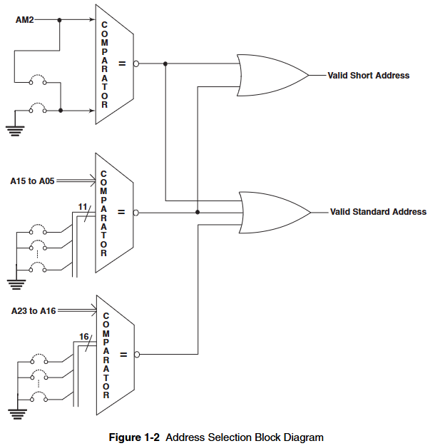
Device Addressing: Supports data transfer in short or standard I/O memory space, with monitoring and/or non privileged data access capabilities. The I/O access type is selected through jumper wires, and the factory defaults to responding to short monitoring I/O access.
VME basic logic: composed of drivers, receivers, and control logic, the DTACK generator is designed to provide high data transmission rates.
Data transmission: The data transmission transceiver supports read and write operations on 8-bit, 16 bit, and 32-bit boundaries.
Register control logic: Supports read and write operations on eight 16 bit bidirectional dual port latches, as well as read operations on CSR registers that control test modes and front panel LEDs. The 128 bit high voltage output can be addressed as four 32-bit long words, eight 16 bit words, or sixteen 8-bit bytes.
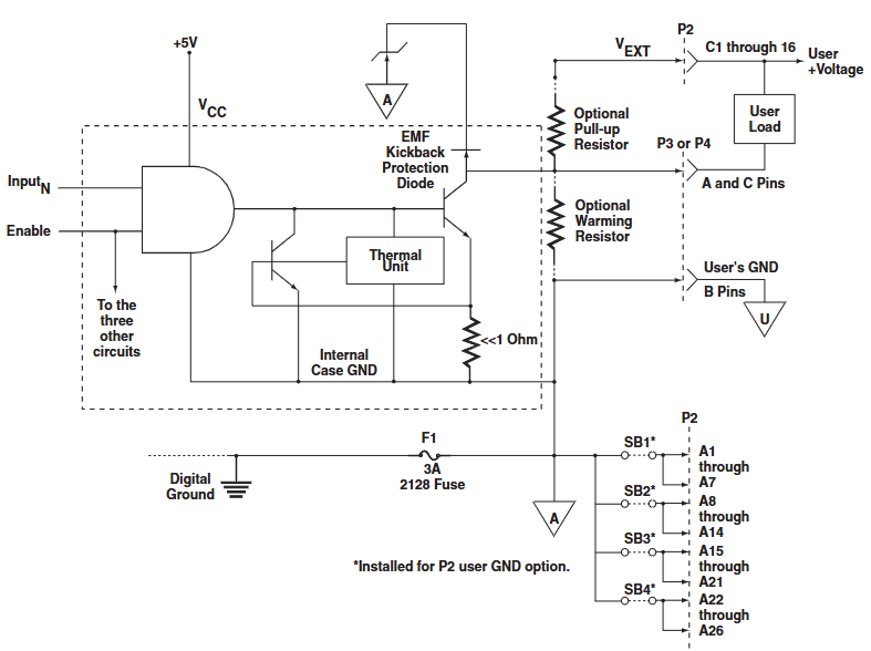
Built in testing (BIT): By enabling the test mode bit in CSR, test data can be written to any output data register (ODR) in test mode and read back during read operations. At this time, all drives are turned off (tri state), and ODR can be read independently of the test mode bit at any time. This function provides real-time loopback testing (when the output driver is connected) and offline diagnostic testing (when the output driver is disconnected from the field device) capabilities. The front panel has a fault LED for quick fault isolation to the board level. The fault LED lights up when powered on or the system is reset, and the user can turn it off after successful diagnosis.
Output driver: Equipped with thermal and surge current shutdown protection, surge current protection allows up to 990mA of surge current before the driver shuts down. If the surge current of each channel in the external circuit exceeds the 990mA limit, preheating resistors should be used. SIP resistor sockets are provided on the board for these preheating resistors, which must be of bus type, with pin 1 as the common terminal and pin 1 of the socket grounded. The power rating of the SIP resistor should be sufficient to handle the required power consumption. The output driver user load return current must provide the lowest possible resistance return path to the user voltage source, and must not be returned through VME backplane digital ground. It must be returned to the user power supply through the B-row pins of the front panel connectors P3 and P4, or through pins A1 to A26 of the P2 connector if the P2 user ground option is ordered. If the user's grounding quality is poor, causing the user's load to return current to the digital grounding of the backplane, fuse F1 will melt and make the board unable to work. A blown fuse usually indicates poor grounding quality for the user, and this fuse circuit is necessary for the digital input grounding return of the control signal to the output driver.
P2 user grounding option: The user grounding is connected to all B-row pins of the front panel connectors P3 and P4. If the P2 user grounding option is ordered, these grounds are also routed to pins A1 to A26 of the backplane P2 connector through the installation of short-circuit bars SB1 to SB4 (RP33 to 36). The external power supply grounding (user grounding) can now be accessed from the P2 backplane connector of the VME chassis. All 26 wires are required to provide a low resistance user load current return path. For a typical 300mA/channel load, the current of each wire can reach up to 1.48A. Each unused wire means that its current must be shared by the remaining wires, so 28 AWG or larger wires should be used.
Configuration and Installation
Unpacking procedure: Some components on GE Fanuc embedded system products may be sensitive to electrostatic discharge. When placing the board on a workbench for configuration and other operations, it is recommended to insert conductive material underneath the board to provide conductive diversion. Unused boards should be stored in their original packaging. After receiving the product, all precautions in the transport container should be followed, all items should be carefully unpacked, and a thorough inspection should be conducted for any transport damage. All claims arising from transport damage should be made to the carrier and a complete report should be sent to the GE Fanuc embedded system, requesting advice on the handling of damaged items.
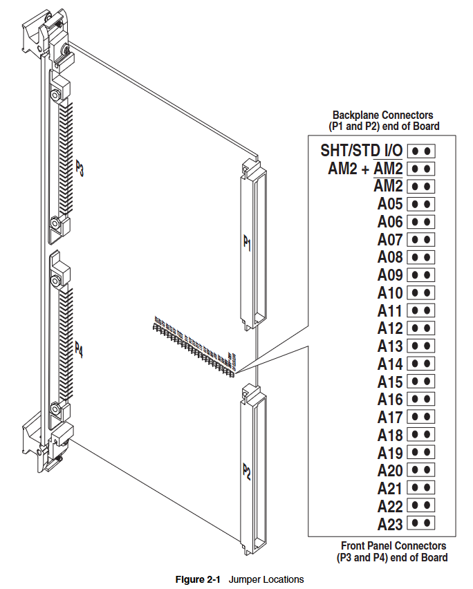
Jumper and switch positions: Introduces the physical positions on the jumper, and the address modifier can change the configuration by installing the jumper at the appropriate position on connector H1, supporting multiple I/O access types. The address selection jumper is used to specify the starting board address for data transmission. The installed jumper is equal to zero, and the omitted jumper is equal to one. The factory default configuration is to respond to 0000 HEX in the short monitoring space.
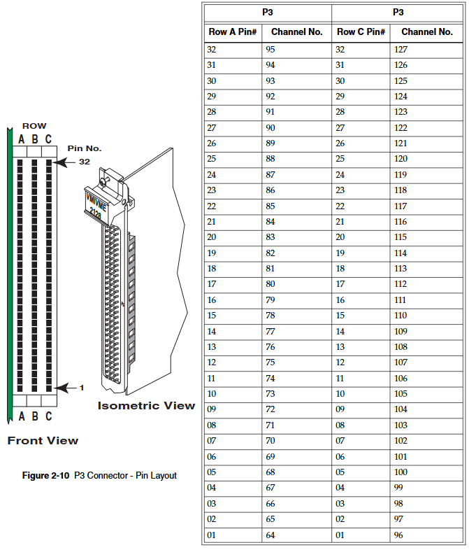
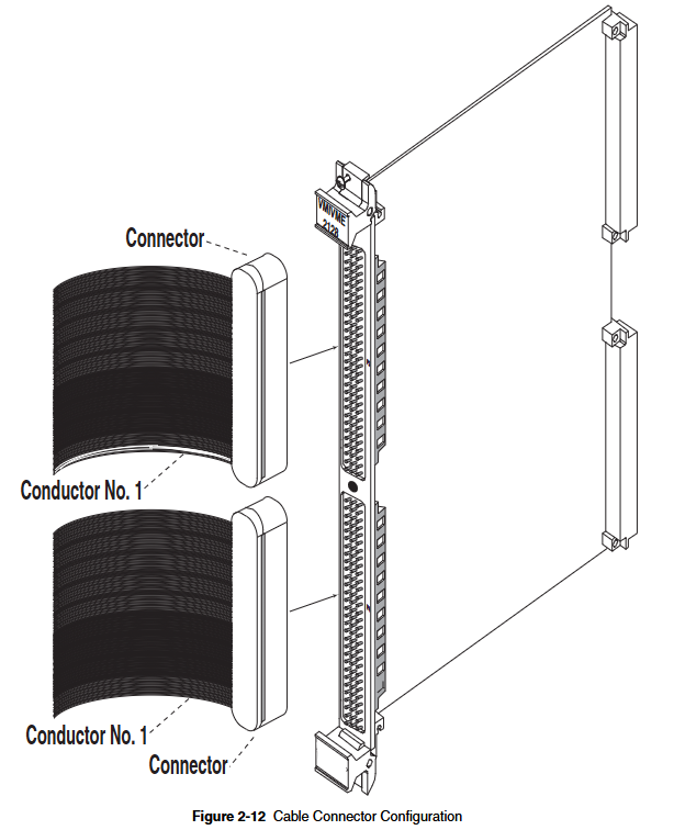
I/O cable and front panel connector configuration: The output connectors (P3 and P4) on VMIVME-2128 are 96 pin DIN standard and can be used with various cables and matching connectors. Users can refer to the relevant application guide for more information. Detailed explanation of the use of user I/O pins and external voltage input for connector P2, as well as the pin configuration of output connectors for P3 and P4. The VMIVME-2128 board is designed with a high-quality ground plane, which is connected to the VME ground through fuse F1 and to the B-row pins on connectors P3 and P4 to enhance noise resistance and improve operational reliability. Users are also reminded that the grounding conductor should be connected to the power supply (GND return) associated with these signal loads, and the grounding connection should prevent excessive current (DC or noise) from flowing through the VME backplane. External user voltage should not be applied to VMIVME-2128 without connecting the VME backplane+5VDC. If these voltages cannot be applied and removed together, the preferred order is: user voltage is connected last and disconnected first.
Optional user grounding: If the user grounding option is ordered, the output return is routed to pins A1 to A26 of P2 through the installation of short-circuit bars SB1 to SB4, allowing access to the external power supply grounding from the P2 backplane of the VME chassis. It is important to maintain the grounding path resistance lower than the VME grounding path resistance and use as many wires as possible to lead out these grounding points. The current in the wires may be large, so 28 AWG or larger wires should be used, while being careful not to exceed the maximum current rating of the connector pins.
Preheating resistor: When the incandescent lamp is initially turned on, the cold filament resistor is the smallest, usually allowing 10 to 12 times the surge current. A surge current of 1A or greater will force the output driver to enter the return current limit. To avoid this problem, preheating or current limiting resistors should be used in the lamp circuit. The preheating resistor should consume about 10% of the rated (hot) current of the bulb. A ten pin SIP socket is provided on the board for preheating resistors, which must be bus type, with pin 1 as the common terminal and pin 1 of the socket grounded. The power rating of the preheating resistor should be sufficient to handle the required power consumption.
Programming
Register Mapping: VMIVME-2128 includes a 16 bit board ID register, a 16 bit CSR, and eight 16 bit ODRs, providing register address mapping. ODRs allow control of 128 high-voltage digital output channels, which can be addressed as four 32-bit long words, eight 16 bit words, or sixteen 8-bit bytes. ODRs can be read under program control for data verification or diagnostic testing. CSR and board ID can be addressed as 16 bit words or two 8-bit bytes, and ID and CSR bit mappings as well as ODR bit mappings are provided. The board uses a 32 byte address space.
Detailed programming: In output data transmission, the data register address mapping displays the correspondence between ODR (DR0 to DR7) and output data channels 127 to 0. The built-in testing function provides real-time loopback data verification and offline diagnostic execution capability. The offline built-in testing function is activated by setting the test mode (TM) bit in CSR to logic "zero". When the TM bit is set, all output drivers are in three states, and test data can be written into the selected data register and read back during read transmission without affecting the user device. When the test mode is turned off, the data can also be read back, allowing online testing of the board. The test mode bit and fault LED control bit are initialized to active state when powered on or system reset, so the fault LED lights up and the output driver is disabled. A simplified programming flowchart is also provided.
Maintenance
When a product malfunctions, it is necessary to first check the software, system configuration, electrical connections, jumper or configuration options, whether the board is fully inserted into its correct connector position, whether the connector pins are clean and free of contaminants, whether there are components or adjacent boards disturbed when inserting or removing the board from the chassis, and the quality of cables and I/O connections.
If you need to return the item, you need to contact GE Fanuc Embedded System to obtain a Return Merchandise Authorization (RMA) number, which can be obtained via email. Customer service can also be contacted by phone or email.
User level maintenance is not recommended, and the drawings and charts in the manual are for reference only.
- YOKOGAWA
- Reliance
- ADVANCED
- SEW
- ProSoft
- WATLOW
- Kongsberg
- FANUC
- VSD
- DCS
- PLC
- man-machine
- Covid-19
- Energy and Gender
- Energy Access
- Renewable Integration
- Energy Subsidies
- Energy and Water
- Net zero emission
- Energy Security
- Critical Minerals
- A-B
- petroleum
- Mine scale
- Sewage treatment
- cement
- architecture
- Industrial information
- New energy
- Automobile market
- electricity
- Construction site
- HIMA
- ABB
- Rockwell
- Schneider Modicon
- Siemens
- xYCOM
- Yaskawa
- Woodward
- BOSCH Rexroth
- MOOG
- General Electric
- American NI
- Rolls-Royce
- CTI
- Honeywell
- EMERSON
- MAN
- GE
- TRICONEX
- Control Wave
- ALSTOM
- AMAT
- STUDER
- KONGSBERG
- MOTOROLA
- DANAHER MOTION
- Bentley
- Galil
- EATON
- MOLEX
- Triconex
- DEIF
- B&W
- ZYGO
- Aerotech
- DANFOSS
- KOLLMORGEN
- Beijer
- Endress+Hauser
- schneider
- Foxboro
- KB
- REXROTH
- YAMAHA
- Johnson
- Westinghouse
- WAGO
- TOSHIBA
- TEKTRONIX
- BENDER
- BMCM
- SMC
- HITACHI
- HIRSCHMANN
- XP POWER
- Baldor
- Meggitt
- SHINKAWA
- Other Brands
- UniOP
- KUKA
- IBA
- Beckhoff
- ADLINK
-
ADLINK HPCI-14S12U - Industrial Control Backplane 12PCI Backplane PCI-14S Passive Backplane
-
ADLINK PCIe-GIE74C - image acquisition card 4-CH GigE Vision PoE+ Frame Grabber
-
ADLINK PCI-8164 - control card 4-Axis Advanced Motion Controller Board
-
ADLINK PCIe-U304 - 4 Port USB3 PCIe Frame Grabbers USB Screw Hole Card
-
ADLINK PCI-9112 - Multi-Function Data Acquisition Card DAQ Card
-
ADLINK PCI-7432 - 51-12013-0A50 4-CH Isolated Numérique I/O PCI Cartes Digital I/O Card
-
ADLINK PCA-6106P3-0C1 REV.C1 - backplane 6-Slot Passive Backplane Board
-
ADLINK PCI-7224 - 24-CH Opto-Isolated Digital I/O PCI Board
-
ADLINK CPCI-7433R(G) - Digital Input Board Rear I/O CompactPCI Card
-
ADLINK EBP-13E4 - 51-46703-0A30 Industrial PC Backplane Passive Backplane
-
ADLINK PCIE-HDV62 - Image acquisition card High Definition Video Frame Grabber
-
ADLINK EBP-13E4 - 51-46703-0A30 Industrial Backplane Board Passive Backplane
-
ADLINK 90111-B1 / CPCI-6770 - PCB CPU MODULE CompactPCI Single Board Computer
-
ADLINK PCI-7248 - DATA ACQUISITION PCI CARD 48-CH Parallel Digital I/O Board
-
ADLINK PCI-7230 - 51-12003-0a50 board PCI7230 32-CH Isolated Digital I/O Card
-
ADLINK PCI2A000CB - 51-20000-0B30 Multi-Function DAQ Card Baseboard
-
ADLINK PCI-8134-005 - 4-Axis Motion Controller Card
-
ADLINK PCI-7224 - 24-CH Opto-Isolated Digital I/O PCI Card
-
ADLINK PCI-7434 - 64-CH Isolated Digital Output Card
-
ADLINK PCI-8132 - motion control card 2-Axis Servo & Stepper Controller
-
ADLINK PCI-8134 - Motion Controller PCI Card 4-Axis Controller Board
-
ADLINK PCI-8164 - Motion Control Card 51-12406-0A40 4-Axis Controller
-
ADLINK 51-12001-0C20 - Circuit Board Data Acquisition Interface Module Hardware
-
ADLINK NuPR0-840 - industrial control motherboard Full-Size PICMG CPU Board
-
ADLINK PCI-7444 - 51-12023-0A10 card 128-CH Isolated Digital Output Board
-
ADLINK PCI-1612B - data acquisition card 4-Port RS-232/422/485 Serial Communication Card
-
ADLINK PCI-6208V 009 - 8/16-CH 16-Bit Analog Output Cards PCB-I-E-482=6BX3
-
ADLINK NUPRO-935A/LV - industrial control motherboard Full-Size PICMG SBC Board
-
ADLINK PCI-9114DG - Multi-Function DAQ Card Data Acquisition PCI Card
-
ADLINK ACL-7130 - Data acquisition card Isolated Digital I/O Board
-
ADLINK ABX-6300D-4E1-BP - board ABX6300D4E1BP Video Interface Expansion Card
-
ADLINK CPCI-6940 - CPCI-6940/D1539/M16-0(EA)-000E 6U CompactPCI Processor Board
-
ADLINK NuPRO-760 - industrial control motherboard Half-Size PICMG SBC CPU Board
-
ADLINK IMB-M42H (G)-0020 - industrial control motherboard LGA1155 Micro-ATX Mainboard
-
ADLINK RTV-24 / PCI-MP4S - 51-12519-1C30 4-Channel Real Time Video Capture Board
-
ADLINK PCI-8134 - 4-Axis Servo & Stepper Motion Controller Card
-
ADLINK MXC-6101D - V.PC000.002.ST.00 Box PC Configurable Embedded Computer
-
ADLINK PCI-8134A - 51-12421-0A10 Motion Control Card 4-Axis Controller Card
-
ADLINK DIN-100S / DIN-100SA1 - Technology SCSI-II TB 100-PIN Terminal Block Board
-
ADLINK DIN-812M001 / DIN812M001 - 51-14034-0A1 51140340A1 Terminal Module Breakout Interface
-
ADLINK PCI-8164 - Servo motion control 4-Axis Advanced Controller Card
-
ADLINK PCIe-GIE64 - Acquisition card GigE Vision PoE+ Frame Grabber
-
ADLINK M-302 - Industrial control motherboard ATX PC Board Mainboard
-
ADLINK PCI-8134 - Motion Controller PCI Card 4-Axis Controller Board
-
ADLINK PCI-RTV24 - Image capture card Analog Video Frame Grabber
-
ADLINK PCI-8102 - Motion control card 2-Axis Servo & Stepper Controller Board
-
ADLINK PCI-9112 REV.B1 - Card Multi-Function Data Acquisition Card
-
ADLINK HSI-DI32-M-N / HSL-TB32-M-DIN - Discrete I/O MODULE Distributed Automation Module System
-
ADLINK PCI-7296 - IO card REV.A3 96-CH Parallel Digital I/O Card
-
ADLINK DIN-814P-A4 / 814Y - terminal board Motion Control Interface Block
-
ADLINK DIN-814P-A4 - 51-14056-0A10 PCB-I-E-2736=ZA01 Screw Terminal Board Breakout
-
ADLINK M-322 - motherboard Industrial Control Computer Mainboard
-
ADLINK NUPRO-406 REV:B1 - industrial control motherboard Full-Size PICMG CPU Board
-
ADLINK AMP-204C - card DSP-Based 4-Axis Advanced Pulse-Train Controller
-
ADLINK HPCI14S REV.B1 - industrial computer baseboard 14-Slot Passive Backplane
-
ADLINK PCI-7250 - 8-CH Relay Output & 8-CH Isolated DI PCI Card
-
ADLINK EBP-13E2 - baseplate Passive Backplane Industrial Computer Chassis Board
-
ADLINK LPCI-3488A - PCI-GPIB card 51-12801-0A30 acquisition card IEEE-488 Interface Board
-
ADLINK PCI-6216V-GL - 51-12201-0C30 16-CH 16-Bit Voltage Analog Output Card
-
ADLINK ACL-8454 - 16-CH Isolated Digital I/O & 4-CH Counter Card
-
ADLINK HPCI-9S7U - backplane Passive Backplane Compatible with NuPRO-A301 852 841 842
-
ADLINK DAQ-2010-007 - Simultaneous-Sampling Multi-Function Data Acquisition Card
-
ADLINK MP-C154 - 51-64205-0A10 Motion Control Card 4-Axis Controller Board
-
ADLINK MXE-202/mSSD16B/WiFi-BT - Matrix Rugged I/O Platform Embedded Fanless Computer
-
ADLINK CM-920-R-17 - PC/104-Plus Single Board Computer Module Intel Celeron M
-
ADLINK PCI-7250 NSMP - 8-CH Relay Output & 8-CH Isolated DI Card
-
ADLINK PCI-8164 - 4-Axis Motion Controller PCI Card W/ Cable and Breakout Box
-
ADLINK EMX-100 - Ethernet-based 4-axis Motion Controllers Distributed Motion Module
-
ADLINK PCI-8134A - Press control card 4-Axis Motion Controller Board
-
ADLINK M-845EG REV:3.2 - industrial motherboard Pentium 4 Socket 478 Micro-ATX
-
ADLINK PCI-9114A Rev A2 DG - card High-Resolution Multi-Function Data Acquisition Board
-
ADLINK IEC-915GV - REV 1.1 Industrial motherboard Socket 478 CPU Board
-
ADLINK PCI-9111DG(G) - Data Acquisition Card Multi-Function DAQ Card
-
ADLINK HPCI-15S10 REV:B2 - Industrial computer base plate Passive Backplane Board
-
ADLINK NuPR0-840 / NuPR0-840DV - industrial control motherboard Full-size PICMG CPU Board
-
ADLINK RTV-24 / PCI-MP4S - 51-12519-1C30 4-Channel Real Time Video Capture Board
-
ADLINK NUPRO-780 - industrial control motherboard Pentium III Single Board Computer
-
ADLINK PCI-7296 - 0050 card 96-CH Opto-Isolated Parallel DIO Card Set
-
ADLINK NUPRO-780 - industrial control motherboard PICMG Full-Size SBC
-
ADLINK PCI-7248 - 51-12006-0A3 002 Pci 7248 48-CH Parallel Digital I/O Card
-
ADLINK PCI-7230 - 32-CH Isolated Digital I/O Card
-
ADLINK AMP-204C - motion control card 4-Axis Advanced Controller Board
-
ADLINK PCI-1714UL - Card Ultra High-Speed 4-CH Simultaneous Sampling DAQ
-
ADLINK NuPRO-E330 - industrial computer equipment motherboard PICMG 1.3 SHB SBC
-
ADLINK AMP-204C - DSP-Based 4-Axis Advanced Pulse-Train Motion Controller Module
-
ADLINK PCI-7256 - 001 51-12206-0A2 REV.A2 LPCI-7256 16-CH Latching Relay Output Card
-
ADLINK ND6050 - NUDAM DIGITAL I/0 MODULE Distributed I/O Unit
-
ASEM BM100 - Box PC Embedded Fanless Industrial Computer
-
ADLINK PCI-7250 - PCI Acquisition Card 8-CH Relay Output & Isolated DI Board
-
ADLINK PCI-8164 - Servo motion control 4-Axis Controller Card
-
ADLINK NuPRO-A40H - Industrial Motherboard 51-41807-1A30 OSP LGA1155 H61
-
ADLINK ADMAX X300 SERVER - 51066010-0A30 motherboard Multi-Processor Mainboard
-
ADLINK CMe-GIE62+ - 51-32903-0A30 control card PC/104-Plus GigE Vision Frame Grabber
-
ADLINK NUPRO-780 - industrial control motherboard Full-Size PICMG SBC CPU Board
-
ADLINK ETX-AT-N270-18/GKTEL - 51-71111-OB10 motherboard ETX CPU Module Board
-
ADLINK DIN-812M - interface module Terminal Block Connection Board
-
ADLINK IMB-M42H - industrial control motherboard LGA1155 Micro-ATX Mainboard
-
ADLINK PXIS-2508 - 8-slot 3U PXI Instrument Chassis Power Hardware Assembly
-
ADLINK AMP-208C - Motion Control card DSP-Based 8-Axis Pulse-Train Controller
-
ADLINK PCI-9111 / PCI-9111DG - Multi-Function Data Acquisition Card DAQ Board
-
ADLINK IEEE-488 GPIB card - Bus Interface Controller Communication Board
-
ADLINK RTV-24 - 51-12519-1C30 image acquisition card Video Frame Grabber Card
-
ADLINK TB-24P/24-01 - Board 24 Way Screw Terminal Breakout Board
-
ADLINK HSL-DI16DO16-DB-NN - 51-23015-0A40 Distributed Discrete I/O Module Set
-
ADLINK PCI-7442 - switch quantity card data acquisition card 64-CH Isolated Card
-
ADLINK ACL-7130 REV. B2 - industrial control capture card Isolated Digital I/O PCI Card
-
ADLINK PCI-6S / PCI6S - Backplane 6-Slot Passive Backplane Chassis Board
-
ADLINK ACL-8113A - card Isolated Digital Input Card
-
ADLINK CPCI-6208V-003 - board cPCI CompactPCI 8-CH Analog Output Card
-
ADLINK DIN-100S-01(G) - SCSI 100-Pin Terminal Block Interface Board
-
ADLINK PCI-7433 - Isolated Digital Input Card 64-CH
-
ADLINK PCI-9812 - Synchronous sampling analog input card High-Speed DAQ Board
-
ADLINK PCI-7434 REV.B1 - PLOTECH PCB-I-E-1182=6EX2 64-CH Isolated Digital Output Card
-
ADLINK PCIe-RTV24 - 51-18016-0A20 4-CH Real-Time Video Capture Card PCIe Frame Grabber
-
ADLINK PCI-8144 / PCI-8144N - Motion control card 4-Axis Stepper Motor Controller
-
ADLINK DIN-68S-01 - terminal board 68-Pin Connector Terminal Block
-
ADLINK MP-C154 - Motion control card 4-Axis Advanced Controller Card
-
ADLINK PCI-7248 (G) - Motherboard 48-CH Parallel Digital I/O Card
-
ADLINK MXE-1301(G) - Intel Atom D2550+NM10 MXE 1300 Series 93-4130-0030 Embedded Computer
-
ADLINK PRO-841 Rev 2.0 / PRO-060907000670 - CPU 2.26GHz & RAM Industrial PC Board
-
ADLINK NuPRO-E330 - Industrial Motherboard System Host Board PICMG 1.3 SHB
-
ADLINK EBP-13E2 - Passive Backplane Industrial Chassis Baseboard
-
ADLINK PCI-8154 - 4-axis Motion Control Card Servo & Stepper Controller Board
-
ADLINK NuPrO-596 REV.B1 - industrial control motherboard Half-size PICMG CPU Board
-
ADLINK PCI-7852 / PCI-7851 - PLOTECH High-Speed Link Control Card Interface Board
-
ADLINK PCI-9112 - 51-12252-0D20 data acquisition card Multi-Function DAQ
-
ADLINK PCI-9112 - Circuit Board 51-12252-0C20 Multi-Function Data Acquisition Card
-
ADLINK NUPRO-761 REV:1.1 - industrial control motherboard PICMG Full-Size CPU Board

K-JIANG

Add: Jimei North Road, Jimei District, Xiamen, Fujian, China
Tell:+86-15305925923