
K-WANG


XYCOM XVME-100 memory module
XYCOM XVME-100 memory module
Product Overview and Core Positioning
Product definition: XYCOM XVME-100 is a single height (3U) VMEbus compatible memory expansion module for industrial control systems, designed to provide RAM, EPROM, mask ROM, or EEPROM storage expansion for VMEbus architecture systems, supporting flexible configuration and data backup.
Core values:
High compatibility: fully compliant with the VMEbus C1 standard, seamlessly integrated into the VMEbus system;
Flexible expansion: Dual storage group design, supporting multiple capacities and types of storage chips, adapting to different scene requirements;
Data security: onboard battery backup and undervoltage protection circuit to prevent data loss caused by power failure;
Independent configuration: Independent settings of storage group address, chip speed, backup power, and other parameters are achieved through jumper wires.
Applicable scenarios: VMEbus architecture devices that require reliable memory expansion, such as industrial automation control, military electronic equipment, embedded systems, etc.
Key specification parameters
(1) Core Performance Parameter Table
Specific specifications of the project
Storage capacity RAM/EPROM/Mask ROM: Maximum 1MB; EEPROM: Maximum 256KB
Design 2 storage groups (Bank1/Bank2), each with 4 32 pin JEDEC slots, supporting independent configuration
Compatible chip specifications and capacities: 8K × 8, 16K × 8, 32K × 8, 64K × 8, 128K × 8 (EEPROM limited to 32K × 8 and below);
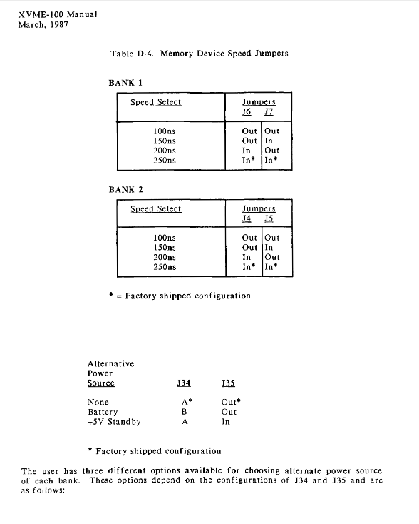
Speed: 100ns, 150ns, 200ns, 250ns
Power requirements: Working power supply:+5V DC (typical 900mA, maximum 1A);
Backup power supply: onboard battery (1.4Ah, typical lifespan of 6 years) or+5V STDBY
Bus compatible with VMEbus C1 standard, A24 address space, DTB slave device
Physical specification 3U Form Factor (single height), size meets VMEbus standard
(2) Environmental and Reliability Parameter Table
Specific specifications of environmental category
Working temperature: 0 ° C~65 ° C (32 ° F~149 ° F)
Storage temperature -40 ° C~85 ° C (-40 ° F~158 ° F)
Humidity 5%~95% RH, non condensing (anti-static protection is required for extremely low humidity)
Altitude work: 0~3048m (10000ft); Storage: 0~15240m (50000ft)
Vibration (working) 5~2000Hz, peak acceleration 10g, peak to peak displacement 0.025mm (maximum)
Impact (working) 30g peak acceleration, 11ms duration
Core functions and design highlights
(1) Storage and configuration functions
Dual storage group independent configuration: Bank1 and Bank2 can set VME address, chip size, address modifier decoding, chip speed, and backup power type separately through jumper wires, supporting mixed use of chips of different specifications;
Multi type storage support: compatible with RAM, EPROM, mask ROM, EEPROM four storage types, EEPROM needs to support fast write/polling technology and TTL logic level;
Flexible allocation of address space: Set the base address through J14-J24 (Bank1) and J16/J26-J33 (Bank2) jumpers, and the address space occupied by the storage group is 4 times the chip capacity, which needs to be aligned to the 4 times capacity boundary.
(2) Data protection mechanism
Undervoltage protection: Equipped with a built-in power monitor, the storage chip is automatically disabled when the+5V voltage is lower than 4.75V to prevent data writing errors. The SYSRESET * drive signal can be optionally enabled;
Dual options for backup power: supports onboard battery backup (compatible with low-power RAM chips) or VMEbus+5V STDBY backup, switched via J34/J35 jumper;
Data anti write design: automatically cuts off the write path of the storage chip in case of power failure, combined with battery backup to ensure long-term storage of RAM data.
(3) Bus and interface characteristics
VMEbus signal compatibility: supports IACKIN */ACKOUT * daisy chain and BUS GRANT signal direct connection, complying with the address, data, and control signal definitions of VMEbus C1 standard;
P1 connector interface: 3-row pin design, including address bus (A01-A23), data bus (D00-D15), control signals (AS *, DS0 */DS1 *, DTACK *, etc.), and power pins;
Status indication: Each storage group is equipped with a green LED that lights up instantly when accessed, providing visual feedback on the working status.
Installation and configuration process
(1) Key items for jumper configuration
Configure Category Jumper Position Core Function
Address/chip size Bank1: J14/J17-J24/J50-J52;
Bank2: J16/J26-J33/J47-J49 Set VME base address (A15-A23) and chip capacity (8K × 8~128K × 8)
Address modifier decoding Bank1: J10-J13;
Bank2: J9/J12/J15 Configure privileged access (super user only/all users), data/program space access permissions
Chip speed selection Bank1: J6-J7;
Bank 2: J4-J5 matching storage chip speed (100ns/150ns/200ns/250ns)
Definition of memory chip pins Bank1: J40-J46;
Bank2: Pin definitions for adapting J2/J3/J25/J36-J39 to different types of storage chips (such as EPROM/RAM pin differences)
Select J34-J35 for backup power and switch between battery backup/+5V STDBY backup/no backup mode
(2) Installation steps
Chip installation: In the power-off state, configure the corresponding jumper according to the storage type, align the storage chip with the slot gap direction, evenly insert it into the 32 pin slot with force, and ensure that the pins are fully in contact;
Rack deployment: Align the module with the VMEbus rack rail, slowly push it in until the connector is fully engaged, and secure the front panel with screws. Each module occupies one 3U slot;
Optional 6U panel installation: If you need to adapt to a 6U rack, you can replace the XVME-945 6U front panel kit and transfer the handle and identification plate according to the manual steps;
Calibrate power monitor: It has been calibrated at the factory. If recalibration is required, adjust the POT R3 potentiometer with a 4.75V reference power supply to ensure accurate triggering threshold for undervoltage protection.
Safety and usage precautions
Battery safety: Short circuit, charging, reverse connection, welding or heating of batteries are prohibited. Waste should be treated as industrial waste to avoid high temperature and contact with metal surfaces;
Static electricity protection: When operating modules and storage chips, it is necessary to release human static electricity, especially CMOS RAM chips are sensitive to static electricity;
Installation taboos: It is forbidden to plug and unplug modules with power on. When inserting, avoid applying too much force to bend the pins and ensure that the module is aligned with the rack rails;
Special requirements for EEPROM: EEPROM must support fast write/polling technology and must use TTL logic level, otherwise it may cause abnormal operation.
- YOKOGAWA
- Reliance
- ADVANCED
- SEW
- ProSoft
- WATLOW
- Kongsberg
- FANUC
- VSD
- DCS
- PLC
- man-machine
- Covid-19
- Energy and Gender
- Energy Access
- Renewable Integration
- Energy Subsidies
- Energy and Water
- Net zero emission
- Energy Security
- Critical Minerals
- A-B
- petroleum
- Mine scale
- Sewage treatment
- cement
- architecture
- Industrial information
- New energy
- Automobile market
- electricity
- Construction site
- HIMA
- ABB
- Rockwell
- Schneider Modicon
- Siemens
- xYCOM
- Yaskawa
- Woodward
- BOSCH Rexroth
- MOOG
- General Electric
- American NI
- Rolls-Royce
- CTI
- Honeywell
- EMERSON
- MAN
- GE
- TRICONEX
- Control Wave
- ALSTOM
- AMAT
- STUDER
- KONGSBERG
- MOTOROLA
- DANAHER MOTION
- Bentley
- Galil
- EATON
- MOLEX
- Triconex
- DEIF
- B&W
- ZYGO
- Aerotech
- DANFOSS
- KOLLMORGEN
- Beijer
- Endress+Hauser
- schneider
- Foxboro
- KB
- REXROTH
- YAMAHA
- Johnson
- Westinghouse
- WAGO
- TOSHIBA
- TEKTRONIX
- BENDER
- BMCM
- SMC
- HITACHI
- HIRSCHMANN
- XP POWER
- Baldor
- Meggitt
- SHINKAWA
- Other Brands
- UniOP
- KUKA
- IBA
- Beckhoff
-
ADLINK CPCI-6860A - 51-31310-OB10 industrial motherboard CompactPCI SBC
-
ADLINK AmITX-SL-G-H110 - 51-7A104-0A30 Mini-ITX Industrial Motherboard
-
ADLINK PXI-2005-003 - CPCI Industrial PC Data Acquisition Card Multi-Function DAQ
-
ADLINK DININ-814M - 51-14032-0A3D SCSI-100P cable connection Interface Terminal Board
-
ADLINK CPCI-3920NA/C2D15/M1G - 3U CompactPCI Intel Core 2 Duo Single Board Computer
-
ADLINK PCIE-8560 - 51-18014-0A20 Communication Card High Speed DAQ
-
ADLINK PCI-C154+ - Motion Control Card 4-axis Motion Controller Board
-
ADLINK PCI-RTV24 - image capture card Analog Video Frame Grabber
-
ADLINK NuPRO-842LV/P - 51-41360-0B30 Industrial Motherboard CPU Board
-
ADLINK cBP-3208/3208R - CPCI Board 3U 8-Slot CompactPCI Backplane
-
ADLINK PCI-8164 - 4-Axis Motion Controller PCI Card 51-12406-0A40
-
ADLINK PCIe-GIE64+ - 4-CH GigE Vision PoE+ Frame Grabber Video Capture Card
-
ADLINK CPCI-6860 / 6860A - CompactPCI Dual Xeon Single Board Computer
-
ADLINK IEC-915GV - REV 1.1 Industrial motherboard CPU Board
-
ADLINK ND-6520 - Technology RS-232 to RS-422RS-485 Converter NuDAM Module
-
ADLINK RTV-24 / PCI-MP4S - 51-12519-1C30 4-Channel Real Time Video Capture Board
-
ADLINK cPCI-6910 / cPCI-6910AM/M1G - cPCI-6910AM/DXL16/M1G/S80G(G)-3120 BOARD CompactPCI SBC
-
ADLINK NUPRO-A40H - Linghua 51-41807-1A30 Industrial Control Computer Motherboard
-
ADLINK USB-3488A - USB to GPIB INTERFACE USB-3488A(G) Controller Module
-
ADLINK PCI-8134A - motion control card 4-Axis Controller Card
-
ADLINK PCI-7432 - Board 32-Channel input / 32-output Isolated Digital I/O PCI Card
-
ADLINK PCI-8134A - 51-12421-0A10 motion controller card tested
-
ADLINK LPCIe-7230 - 32 CH Isolated Input/output Card 2 Interrupts Low Profile PCIe
-
ADLINK NuPRO-E340 - industrial computer motherboard 51-47807-0A30 PICMG 1.3 SHB
-
ADLINK PCI-7434 - High-speed Digital Acquisition Card 64-CH Isolated DO Card
-
ADLINK NuPRO-E330 - 51-41805-0A20 Indsutrial Board SHB Single Board Computer
-
ADLINK PCI-7248 - OPTO-22 48 CHANNEL DIO DIGITAL TTL/DTL I/O 51-12006-0A40 GP
-
ADLINK PCI-8134 - Motion control card 4-Axis Controller Card
-
ADLINK AMP-208C - Movimiento Control Tarjeta 51-12420-1A20 W/Expansión & Breakout
-
ADLINK PCI-8164 - 51-12406-0A40 PCB Board 4-Axis Motion Controller Card
-
ADLINK DIN-68Y-SGII / DIN-68M-J3A - Terminal Board Connector Interface Block
-
ADLINK PCIe-7432 - Technology 51-18402-0A10 PCIe Card With High Input Range
-
ADLINK PCI-8144 / PCI-8144N - Motion control card 4-Axis Stepper Controller Card
-
ADLINK HSL-HUB3/REPEATER - HIGH SPEED LINK EXTENSION MODULES Distributed Hub Module
-
ADLINK ND-6017 - Data Logging + Acquisition 8CH A/D input Mod NuDAM Module
-
ADLINK LPCIe-7250 - data acquisition card Low Profile 8-CH Relay Output Card
-
ADLINK PCI-7432 - I/O card 64-CH Isolated Digital Input Output PCI Card
-
ADLINK IMB-M43H - industrial control computer motherboard Q87 Chip Micro-ATX
-
ADLINK MP-C154 - Motion control Card 4-Axis Motion Controller Board
-
ADLINK PCI-RTV24 - image capture card Video Frame Grabber Card
-
ADLINK PCI-7250 - 8-CH Relay Output & 8-CH Isolated DI Card
-
ADLINK PCI-6308V - 8-CH 12-Bit Isolated Analog Output PCI Card PCB-I-E-1148=6EX2
-
ADLINK PCI-7248 - capture card 48-CH Opto-22 Compatible DIO Card
-
ADLINK HSL-AI16A02-M-VV - Analog Input Output Distributed Module
-
ADLINK NuPRO-A301 - Rev:1.4 NUPRO-A301 PICMG Full-Size Single Board Computer
-
ADLINK PCI-6208V-GL - 8-CH Voltage Analog Output PCI Card
-
ADLINK PCI-8134A - 51-12421-0A10 4-Axis Motion Controller Card
-
ADLINK MNET-S23 - TECHNOLOGY MNET S23 - SERVO DRIVER CONTROL MODULE
-
ADLINK M-342 - ATX I3 I5 I7 Q67 Industrial Motherboard
-
ADLINK NUPRO-780 - Industrial Motherboard CPU Board PICMG SBC
-
ADLINK MP-C154 / MP-C152 - 4-Axis Motion Control Card Pulse-Train Controller
-
ADLINK NuPRO-935A/LV10B0 - Motherboard 51-41802-0A10 GP w/RAM Industrial Control Board
-
ADLINK MP-C154 - Motion control card 4-Axis Motion Controller Mainboard
-
ADLINK PCI-7250 - PCI Acquisition Card 8-CH Relay Output Isolated DI Card
-
ADLINK ACL-7124 - Technology Inc.24 DIO Card Digital Input Output Card
-
ADLINK PCI-8554 A2 - Timer/Counter Data Acquisition Card
-
ADLINK DIN-825-GP4 - Terminal Block Interface Board Breakout Module
-
ADLINK NuPR0-761 - REV:1.1 Industrial motherboard Full-Size PICMG SBC
-
ADLINK MXE-1401/M8G (G) - Matrix Fanless Embedded Computer Industrial PC
-
ADLINK HSL-DI16DO16-UD-NN - Digital 16 Channel I/O Mod Distributed I/O Module
-
ADLINK ND6520 - NUDAM INTELLIGENT DA&C MODULE RS232-RS-422/RS485 CONVERTOR
-
ADLINK NUPRO-761 - REV:1.1 Industrial Motherboard CPU Board
-
ADLINK AMP-208C - Motion Control Card 51-12420-1A20 DSP-based 8-axis
-
ADLINK NuPRO-A301REV 1.4 - with packaging industrial computer motherboard PICMG SBC
-
ADLINK PCM-9112+ - 51-12300-0A2 industrial motherboard Multi-Function DAQ PC/104 Module
-
ADLINK PCM-7250+ - 8-CH Relay Outputs & 8-CH Isolated DI Module PC/104
-
ADLINK PCI-RTV24 - Image capture card Analog Video Frame Grabber
-
ADLINK PCI-8134 - Motion Controller PCI Card 4-Axis Controller Board
-
ADLINK PCI-7432 - Isolated Digital I/O PCI Card
-
ADLINK PCI-8554 A2 - acquisition card Timer/Counter Card
-
ADLINK PCI-8132 - Rev.A2 2-Axis Servo & Stepper Motion Controller Card
-
ADLINK PCI-8132 - Data Acquisition card 2-Axis Motion Controller Card
-
ADLINK EBP-13E4 - 51-46703-0A30 Industrial Backplane Board Passive Backplane
-
ADLINK PCI-800L - Electronic Card Interface Controller Card
-
ADLINK PCIe-GIE72 - 51-18531-0A10 PCB Board GigE Vision Frame Grabber
-
ADLINK DAQ-2010(G)-OOBO - Simultaneous-Sampling Multi-Function DAQ Card
-
ADLINK PCI-9112 - REV.B1 Multifunction DAQ Card Data Acquisition Card
-
ADLINK PCI-7230 - 51-12003-DA60 32-CH Isolated Digital I/O Card
-
ADLINK PCI-7432 - Data Acquisition Card Isolated Digital I/O PCI Card
-
ADLINK ETX-AT-N270-18/LXE - 51-71111-0A20 ETX CPU Module Motherboard
-
ADLINK HSL-DI32-UD-N - DIGITAL INPUT 32 POINTS MODULE Distributed I/O
-
ADLINK AMP-204C - Motion Control card DSP-Based 4-Axis Advanced Controller
-
ADLINK MNET-4XMOG-0050 - Four-axis Motion Controller Distributed Motion Module
-
ADLINK AMP-204C - Motion control card DSP-Based 4-Axis Pulse-Train Controller
-
ADLINK PCI-7442 - Switch card 64-Channel Datalogging & Acquisition Card
-
ADLINK M-302 - Industrial control motherboard ATX PC Board
-
ADLINK NUPRO-852 / NUPRO-852LV - Industrial motherboard Single Board Computer
-
ADLINK PCI-8134 - REV.B1. 4-Axis Motion Controller Card
-
ADLINK PCI-GIE62 + - 51-18502-0A20 2-CH GigE Vision Frame Grabber PoE Card
-
ADLINK PCI-MPG24 - 51-12523-0B20 MPEG4 Card Video Compression Hardware
-
ADLINK HSL-TB32-M-DIN - 32-CH I/O TERMINAL W/ HSL-AI16AO2-M-VV MODULE
-
ADLINK PCI-M114-GL - PCB Ver 2.1 Motion Controller Axis Card
-
ADLINK IMB-M40H - SYM76996H61 motherboard Industrial Computer Mainboard
-
ADLINK NUPRO-A40H - 51-41807-1A20 industrial control motherboard H61 Chip
-
ADLINK PCI-M114-GL - Axis Card Data Acquisition Card PCB VER2.2 Motion Controller
-
ADLINK PCI-8134 - Motion Controller PCI Card 4-Axis Controller Board
-
ADLINK PCI-8102 - Motion control card 2-Axis Servo & Stepper Controller
-
ADLINK NuPRO-841REV:3.0 - motherboard Industrial Control PC Board
-
ADLINK HSL-TB32-U-DIN REV A1 - Breakout Terminal Board Field I/O Module
-
ADLINK AMP-204C - Motion Control card DSP-Based 4-Axis Pulse-Train Controller
-
ADLINK NUPRO-A40H - 51-41807-1A20 industrial control motherboard H61 PC Board
-
ADLINK PCI-6308A / PCI-6308V - 51-12202-0A50 Isolated Analog Output Card
-
ADLINK AMP-204C - DSP-Based 4-Axis Advanced Pulse-Train Motion Controller
-
ADLINK PCI-7434 - Technology 64-Channel Isolated Digital I/O PCI Cards
-
ADLINK CPCI-6840 / CPCI-6840V / PM16/M1G-12G0 - CompactPCI Single Board Computer CPU Module
-
ADLINK PCIE-GIE74 - Motherboard Video Capture Card 51-18531-0A10 Frame Grabber
-
ADLINK NuPRO-E330 - industrial computer equipment motherboard Control Mainboard
-
ADLINK AMP-208C / 51-12420-1A20 - Motion Control Card W/ Expansion & Breakout Board
-
ADLINK HPCI-14S12U - industrial computer baseboard Passive Backplane 14 Slots
-
ADLINK PCI-8164 - 4-Axis Motion Controller PCI Card W/ 1x Cable, 1x Breakout Box
-
ADLINK PCIe-RTV24 - 51-18016-0A20 Image Acquisition Video Capture Card
-
ADLINK M-342 - 5 PCI ATX Motherboard Industrial PC Mainboard
-
ADLINK PCI-FIW64 - 4/2 Channel IEEE1394B Image Capture Card FireWire Frame Grabber
-
ADLINK PCI-7432 - digital IO card 64-CH Isolated Digital Input Output Card
-
ADLINK 51-12001-0C20 - Circuit Board PCI-7200 Data Acquisition Controller Card
-
ADLINK PXI-3920 - PXI 3U cPCI Industrial Controller Embedded System CPU Board
-
ADLINK NuPRO-841REV:2.0 - motherboard Industrial Control PC Board
-
ADLINK NuPro-E330 - 51-41805-0A20 PCB Industrial Control Computer Motherboard
-
ADLINK PCI-RTV24 - Image capture card Analog Video Frame Grabber
-
ADLINK PCI-7442 - Switch card 64-Channel Datalogging & Acquisition Card
-
ADLINK HPX-13S4 - device baseboard Passive Backplane Riser Card
-
ADLINK PCI-9112 REV A.1 - Multi Function DA&C Board Data Acquisition Card
-
ADLINK PCI-7248 - 51-12006-0A40 Card Control 48-CH Digital I/O Module
-
ADLINK CPCI-6860 / 6860A - motherboard CompactPCI Dual Xeon Single Board Computer
-
ADLINK DPAC-3020-11(G) - Embedded PC Automation Controller Machine Control Board
-
ADLINK NuPRO-841 REV:1.0 - industrial control motherboard CPU Board
-
ADLINK MNET-4XMOG-0050 - Four-axis Motion Controller MNET Motion Control Card
-
ADLINK ETX-AT-N270-18/LXE - 51-71111-0A20 ETX CPU Module Motherboard

K-JIANG

Add: Jimei North Road, Jimei District, Xiamen, Fujian, China
Tell:+86-15305925923