
K-WANG
+086-15305925923
Service expert in industrial control field!


Product
Article
NameDescriptionContent
Adequate Inventory, Timely Service
pursuit of excellence


Ship control system
Equipment control system
Power monitoring system
Current position:
新闻动态
newS
Brand
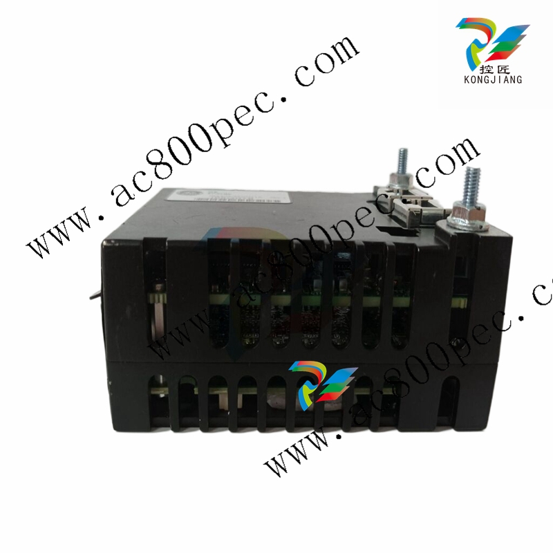
GE IS220PAOCH1A Analog output: 8, 0-20 mA output
GE IS220PAOCH1A Analog output: 8, 0-20 mA output
GE IS220PAOCH1A Analog output: 8, 0-20 mA output
The MAX6659MEE can be monitored and controlled on the SMBus at address
0x98 for the V7768/V7769. This will allow the user to monitor and set up the
alarm (OVERT2).
For more information on the Maxim MAX6659MEE contact them directly at:
1-888-629-4642, or visit Maxim’s website at www.maxim-ic.com.
3.2 Embedded PCI Functions
The V7768/V7769 provide non-volatile RAM (NVRAM), timers and a Watchdog
Timer via the PCI bus FPGA. These functions are required for embedded and real
time applications. The PCI configuration space of these embedded functions is
shown in Table 3-1.
Table 3-1 PCI Configuration Space Registers
31 16 15 0 Register Address
Device ID 0004 Vendor ID 114A 00h
Status Command 04h
Class Code Revision ID 08h
BIST Header Type Latency Timer Cache Line Size 0Ch
PCI Base Address 0 for Memory-Mapped VME Control registers (BAR0) 10h
PCI Base Address 1 for Memory-Mapped 32 KByte NVRAM (BAR1) 14h
PCI Base Address 2 for Memory Mapped Watchdog and other timers (BAR2) 18h
Reserved 1Ch
Reserved 20h
Reserved 24h
Reserved 28h
Subsystem ID 7768 Subsystem Vendor ID 114A 2Ch
Reserved 30h
Reserved 34h
Reserved 38h
Max_Lat Min_gnt Interrupt Pin Interrupt Line 3Ch
The “Device ID” field indicates that the device is for VME products (00) and
indicates the supported embedded feature set.
The “Vendor ID” and “Subsystem Vendor ID” fields indicate GE’s PICMG®
assigned Vendor ID (114A).
The “Subsystem ID” field indicates the model number of the product (7768).
The V7768/V7769 provide four user-programmable timers (two 16-bit and two
32-bit) which are completely dedicated to user applications and are not required
for any standard system function. Each timer is clocked by independent
generators with selectable rates of 2 MHz, 1 MHz, 500 kHz and 250 kHz. Each
timer may be independently enabled and each is capable of generating a system
interrupt on timeout.
Events can be timed by either polling the timers or enabling the interrupt
capability of the timer. A status register allows for application software to
determine which timer is the cause of any interrupt.
3.3.1 Timer Control Status Register 1 (TCSR1)
The timers are controlled and monitored via the Timer Control Status Register 1
(TCSR1) located at offset 0x00 from the address in BAR2. The mapping of the bits
in this register are shown in Table 3-2.
Table 3-2 TCSR1 Bit Mapping
Field Bits Read or Write
Timer 1 Caused IRQ TCSR1[0] R/W
Timer 1 Enable TCSR1[1] R/W
Timer 1 IRQ Enable TCSR1[2] R/W
Timer 1 Clock Select TCSR1[4..3] R/W
Timer 2 Caused IRQ TCSR1[8] R/W
Timer 2 Enable TCSR1[9] R/W
Timer 2 IRQ Enable TCSR1[10] R/W
Timer 2 Clock Select TCSR1[12..11] R/W
Timer 3 Caused IRQ TCSR1[16] R/W
Timer 3 Enable TCSR1[17] R/W
Timer 3 IRQ Enable TCSR1[18] R/W
Timer 3 Clock Select TCSR1[20..19] R/W
Timer 4 Caused IRQ TCSR1[24] R/W
Timer 4 Enable TCSR1[25] R/W
Timer 4 IRQ Enable TCSR1[26] R/W
Timer 4 Clock Select TCSR1[28..27] R/W
Reserved All Other Bits R/W
All of these bits default to “0” after system reset.
Each timer has an independently selectable clock source which is selected by the
bit pattern in the “Timer x Clock Select” field as shown in Table 3-3.
Table 3-3 Selectable Clock Source for Timers
Clock Ratio MSb LSb
2 MHz 0 0
1 MHz 0 1
500 kHz 1 0
250 kHz 1 1
- YOKOGAWA
- Reliance
- ADVANCED
- SEW
- ProSoft
- WATLOW
- Kongsberg
- FANUC
- VSD
- DCS
- PLC
- man-machine
- Covid-19
- Energy and Gender
- Energy Access
- Renewable Integration
- Energy Subsidies
- Energy and Water
- Net zero emission
- Energy Security
- Critical Minerals
- A-B
- petroleum
- Mine scale
- Sewage treatment
- cement
- architecture
- Industrial information
- New energy
- Automobile market
- electricity
- Construction site
- HIMA
- ABB
- Rockwell
- Schneider Modicon
- Siemens
- xYCOM
- Yaskawa
- Woodward
- BOSCH Rexroth
- MOOG
- General Electric
- American NI
- Rolls-Royce
- CTI
- Honeywell
- EMERSON
- MAN
- GE
- TRICONEX
- Control Wave
- ALSTOM
- AMAT
- STUDER
- KONGSBERG
- MOTOROLA
- DANAHER MOTION
- Bentley
- Galil
- EATON
- MOLEX
- Triconex
- DEIF
- B&W
- ZYGO
- Aerotech
- DANFOSS
- KOLLMORGEN
- Beijer
- Endress+Hauser
- schneider
- Foxboro
- KB
- REXROTH
- YAMAHA
- Johnson
- Westinghouse
- WAGO
- TOSHIBA
- TEKTRONIX
- BENDER
- BMCM
- SMC
- HITACHI
- HIRSCHMANN
- XP POWER
- Baldor
- Meggitt
- SHINKAWA
- Other Brands
- UniOP
- KUKA
- IBA
- Beckhoff
- ADLINK
91
-
ADLINK HPCI-14S12U - Industrial Control Backplane 12PCI Backplane PCI-14S Passive Backplane
-
ADLINK PCIe-GIE74C - image acquisition card 4-CH GigE Vision PoE+ Frame Grabber
-
ADLINK PCI-8164 - control card 4-Axis Advanced Motion Controller Board
-
ADLINK PCIe-U304 - 4 Port USB3 PCIe Frame Grabbers USB Screw Hole Card
-
ADLINK PCI-9112 - Multi-Function Data Acquisition Card DAQ Card
-
ADLINK PCI-7432 - 51-12013-0A50 4-CH Isolated Numérique I/O PCI Cartes Digital I/O Card
-
ADLINK PCA-6106P3-0C1 REV.C1 - backplane 6-Slot Passive Backplane Board
-
ADLINK PCI-7224 - 24-CH Opto-Isolated Digital I/O PCI Board
-
ADLINK CPCI-7433R(G) - Digital Input Board Rear I/O CompactPCI Card
-
ADLINK EBP-13E4 - 51-46703-0A30 Industrial PC Backplane Passive Backplane
-
ADLINK PCIE-HDV62 - Image acquisition card High Definition Video Frame Grabber
-
ADLINK EBP-13E4 - 51-46703-0A30 Industrial Backplane Board Passive Backplane
-
ADLINK 90111-B1 / CPCI-6770 - PCB CPU MODULE CompactPCI Single Board Computer
-
ADLINK PCI-7248 - DATA ACQUISITION PCI CARD 48-CH Parallel Digital I/O Board
-
ADLINK PCI-7230 - 51-12003-0a50 board PCI7230 32-CH Isolated Digital I/O Card
-
ADLINK PCI2A000CB - 51-20000-0B30 Multi-Function DAQ Card Baseboard
-
ADLINK PCI-8134-005 - 4-Axis Motion Controller Card
-
ADLINK PCI-7224 - 24-CH Opto-Isolated Digital I/O PCI Card
-
ADLINK PCI-7434 - 64-CH Isolated Digital Output Card
-
ADLINK PCI-8132 - motion control card 2-Axis Servo & Stepper Controller
-
ADLINK PCI-8134 - Motion Controller PCI Card 4-Axis Controller Board
-
ADLINK PCI-8164 - Motion Control Card 51-12406-0A40 4-Axis Controller
-
ADLINK 51-12001-0C20 - Circuit Board Data Acquisition Interface Module Hardware
-
ADLINK NuPR0-840 - industrial control motherboard Full-Size PICMG CPU Board
-
ADLINK PCI-7444 - 51-12023-0A10 card 128-CH Isolated Digital Output Board
-
ADLINK PCI-1612B - data acquisition card 4-Port RS-232/422/485 Serial Communication Card
-
ADLINK PCI-6208V 009 - 8/16-CH 16-Bit Analog Output Cards PCB-I-E-482=6BX3
-
ADLINK NUPRO-935A/LV - industrial control motherboard Full-Size PICMG SBC Board
-
ADLINK PCI-9114DG - Multi-Function DAQ Card Data Acquisition PCI Card
-
ADLINK ACL-7130 - Data acquisition card Isolated Digital I/O Board
-
ADLINK ABX-6300D-4E1-BP - board ABX6300D4E1BP Video Interface Expansion Card
-
ADLINK CPCI-6940 - CPCI-6940/D1539/M16-0(EA)-000E 6U CompactPCI Processor Board
-
ADLINK NuPRO-760 - industrial control motherboard Half-Size PICMG SBC CPU Board
-
ADLINK IMB-M42H (G)-0020 - industrial control motherboard LGA1155 Micro-ATX Mainboard
-
ADLINK RTV-24 / PCI-MP4S - 51-12519-1C30 4-Channel Real Time Video Capture Board
-
ADLINK PCI-8134 - 4-Axis Servo & Stepper Motion Controller Card
-
ADLINK MXC-6101D - V.PC000.002.ST.00 Box PC Configurable Embedded Computer
-
ADLINK PCI-8134A - 51-12421-0A10 Motion Control Card 4-Axis Controller Card
-
ADLINK DIN-100S / DIN-100SA1 - Technology SCSI-II TB 100-PIN Terminal Block Board
-
ADLINK DIN-812M001 / DIN812M001 - 51-14034-0A1 51140340A1 Terminal Module Breakout Interface
-
ADLINK PCI-8164 - Servo motion control 4-Axis Advanced Controller Card
-
ADLINK PCIe-GIE64 - Acquisition card GigE Vision PoE+ Frame Grabber
-
ADLINK M-302 - Industrial control motherboard ATX PC Board Mainboard
-
ADLINK PCI-8134 - Motion Controller PCI Card 4-Axis Controller Board
-
ADLINK PCI-RTV24 - Image capture card Analog Video Frame Grabber
-
ADLINK PCI-8102 - Motion control card 2-Axis Servo & Stepper Controller Board
-
ADLINK PCI-9112 REV.B1 - Card Multi-Function Data Acquisition Card
-
ADLINK HSI-DI32-M-N / HSL-TB32-M-DIN - Discrete I/O MODULE Distributed Automation Module System
-
ADLINK PCI-7296 - IO card REV.A3 96-CH Parallel Digital I/O Card
-
ADLINK DIN-814P-A4 / 814Y - terminal board Motion Control Interface Block
-
ADLINK DIN-814P-A4 - 51-14056-0A10 PCB-I-E-2736=ZA01 Screw Terminal Board Breakout
-
ADLINK M-322 - motherboard Industrial Control Computer Mainboard
-
ADLINK NUPRO-406 REV:B1 - industrial control motherboard Full-Size PICMG CPU Board
-
ADLINK AMP-204C - card DSP-Based 4-Axis Advanced Pulse-Train Controller
-
ADLINK HPCI14S REV.B1 - industrial computer baseboard 14-Slot Passive Backplane
-
ADLINK PCI-7250 - 8-CH Relay Output & 8-CH Isolated DI PCI Card
-
ADLINK EBP-13E2 - baseplate Passive Backplane Industrial Computer Chassis Board
-
ADLINK LPCI-3488A - PCI-GPIB card 51-12801-0A30 acquisition card IEEE-488 Interface Board
-
ADLINK PCI-6216V-GL - 51-12201-0C30 16-CH 16-Bit Voltage Analog Output Card
-
ADLINK ACL-8454 - 16-CH Isolated Digital I/O & 4-CH Counter Card
-
ADLINK HPCI-9S7U - backplane Passive Backplane Compatible with NuPRO-A301 852 841 842
-
ADLINK DAQ-2010-007 - Simultaneous-Sampling Multi-Function Data Acquisition Card
-
ADLINK MP-C154 - 51-64205-0A10 Motion Control Card 4-Axis Controller Board
-
ADLINK MXE-202/mSSD16B/WiFi-BT - Matrix Rugged I/O Platform Embedded Fanless Computer
-
ADLINK CM-920-R-17 - PC/104-Plus Single Board Computer Module Intel Celeron M
-
ADLINK PCI-7250 NSMP - 8-CH Relay Output & 8-CH Isolated DI Card
-
ADLINK PCI-8164 - 4-Axis Motion Controller PCI Card W/ Cable and Breakout Box
-
ADLINK EMX-100 - Ethernet-based 4-axis Motion Controllers Distributed Motion Module
-
ADLINK PCI-8134A - Press control card 4-Axis Motion Controller Board
-
ADLINK M-845EG REV:3.2 - industrial motherboard Pentium 4 Socket 478 Micro-ATX
-
ADLINK PCI-9114A Rev A2 DG - card High-Resolution Multi-Function Data Acquisition Board
-
ADLINK IEC-915GV - REV 1.1 Industrial motherboard Socket 478 CPU Board
-
ADLINK PCI-9111DG(G) - Data Acquisition Card Multi-Function DAQ Card
-
ADLINK HPCI-15S10 REV:B2 - Industrial computer base plate Passive Backplane Board
-
ADLINK NuPR0-840 / NuPR0-840DV - industrial control motherboard Full-size PICMG CPU Board
-
ADLINK RTV-24 / PCI-MP4S - 51-12519-1C30 4-Channel Real Time Video Capture Board
-
ADLINK NUPRO-780 - industrial control motherboard Pentium III Single Board Computer
-
ADLINK PCI-7296 - 0050 card 96-CH Opto-Isolated Parallel DIO Card Set
-
ADLINK NUPRO-780 - industrial control motherboard PICMG Full-Size SBC
-
ADLINK PCI-7248 - 51-12006-0A3 002 Pci 7248 48-CH Parallel Digital I/O Card
-
ADLINK PCI-7230 - 32-CH Isolated Digital I/O Card
-
ADLINK AMP-204C - motion control card 4-Axis Advanced Controller Board
-
ADLINK PCI-1714UL - Card Ultra High-Speed 4-CH Simultaneous Sampling DAQ
-
ADLINK NuPRO-E330 - industrial computer equipment motherboard PICMG 1.3 SHB SBC
-
ADLINK AMP-204C - DSP-Based 4-Axis Advanced Pulse-Train Motion Controller Module
-
ADLINK PCI-7256 - 001 51-12206-0A2 REV.A2 LPCI-7256 16-CH Latching Relay Output Card
-
ADLINK ND6050 - NUDAM DIGITAL I/0 MODULE Distributed I/O Unit
-
ASEM BM100 - Box PC Embedded Fanless Industrial Computer
-
ADLINK PCI-7250 - PCI Acquisition Card 8-CH Relay Output & Isolated DI Board
-
ADLINK PCI-8164 - Servo motion control 4-Axis Controller Card
-
ADLINK NuPRO-A40H - Industrial Motherboard 51-41807-1A30 OSP LGA1155 H61
-
ADLINK ADMAX X300 SERVER - 51066010-0A30 motherboard Multi-Processor Mainboard
-
ADLINK CMe-GIE62+ - 51-32903-0A30 control card PC/104-Plus GigE Vision Frame Grabber
-
ADLINK NUPRO-780 - industrial control motherboard Full-Size PICMG SBC CPU Board
-
ADLINK ETX-AT-N270-18/GKTEL - 51-71111-OB10 motherboard ETX CPU Module Board
-
ADLINK DIN-812M - interface module Terminal Block Connection Board
-
ADLINK IMB-M42H - industrial control motherboard LGA1155 Micro-ATX Mainboard
-
ADLINK PXIS-2508 - 8-slot 3U PXI Instrument Chassis Power Hardware Assembly
-
ADLINK AMP-208C - Motion Control card DSP-Based 8-Axis Pulse-Train Controller
-
ADLINK PCI-9111 / PCI-9111DG - Multi-Function Data Acquisition Card DAQ Board
-
ADLINK IEEE-488 GPIB card - Bus Interface Controller Communication Board
-
ADLINK RTV-24 - 51-12519-1C30 image acquisition card Video Frame Grabber Card
-
ADLINK TB-24P/24-01 - Board 24 Way Screw Terminal Breakout Board
-
ADLINK HSL-DI16DO16-DB-NN - 51-23015-0A40 Distributed Discrete I/O Module Set
-
ADLINK PCI-7442 - switch quantity card data acquisition card 64-CH Isolated Card
-
ADLINK ACL-7130 REV. B2 - industrial control capture card Isolated Digital I/O PCI Card
-
ADLINK PCI-6S / PCI6S - Backplane 6-Slot Passive Backplane Chassis Board
-
ADLINK ACL-8113A - card Isolated Digital Input Card
-
ADLINK CPCI-6208V-003 - board cPCI CompactPCI 8-CH Analog Output Card
-
ADLINK DIN-100S-01(G) - SCSI 100-Pin Terminal Block Interface Board
-
ADLINK PCI-7433 - Isolated Digital Input Card 64-CH
-
ADLINK PCI-9812 - Synchronous sampling analog input card High-Speed DAQ Board
-
ADLINK PCI-7434 REV.B1 - PLOTECH PCB-I-E-1182=6EX2 64-CH Isolated Digital Output Card
-
ADLINK PCIe-RTV24 - 51-18016-0A20 4-CH Real-Time Video Capture Card PCIe Frame Grabber
-
ADLINK PCI-8144 / PCI-8144N - Motion control card 4-Axis Stepper Motor Controller
-
ADLINK DIN-68S-01 - terminal board 68-Pin Connector Terminal Block
-
ADLINK MP-C154 - Motion control card 4-Axis Advanced Controller Card
-
ADLINK PCI-7248 (G) - Motherboard 48-CH Parallel Digital I/O Card
-
ADLINK MXE-1301(G) - Intel Atom D2550+NM10 MXE 1300 Series 93-4130-0030 Embedded Computer
-
ADLINK PRO-841 Rev 2.0 / PRO-060907000670 - CPU 2.26GHz & RAM Industrial PC Board
-
ADLINK NuPRO-E330 - Industrial Motherboard System Host Board PICMG 1.3 SHB
-
ADLINK EBP-13E2 - Passive Backplane Industrial Chassis Baseboard
-
ADLINK PCI-8154 - 4-axis Motion Control Card Servo & Stepper Controller Board
-
ADLINK NuPrO-596 REV.B1 - industrial control motherboard Half-size PICMG CPU Board
-
ADLINK PCI-7852 / PCI-7851 - PLOTECH High-Speed Link Control Card Interface Board
-
ADLINK PCI-9112 - 51-12252-0D20 data acquisition card Multi-Function DAQ
-
ADLINK PCI-9112 - Circuit Board 51-12252-0C20 Multi-Function Data Acquisition Card
-
ADLINK NUPRO-761 REV:1.1 - industrial control motherboard PICMG Full-Size CPU Board

K-JIANG

Add: Jimei North Road, Jimei District, Xiamen, Fujian, China
Tell:+86-15305925923