
K-WANG


MOTOROLA MVME162 Embedded Controller
MOTOROLA MVME162 Embedded Controller
The complete user guide for the Motorola MVME162 series embedded controller (model 001-043) is developed from eight dimensions: manual basic information, hardware specifications, hardware configuration installation, operating instructions, functional modules, serial port interconnection, security compliance, and supporting resources. It is the core reference for the design, use, and development of this controller. The following is a detailed summary of the points:
Core hardware specifications
MVME162 is a dual high VME module, divided into 21 models (001-043). The core configuration revolves around a 25MHz 32-bit MC68LC040/MC68040 processor, both of which include 8KB cache and MMU. MC68040 also comes with a floating point coprocessor (FPU). The differences in core capacity among different models are DRAM capacity and whether they have SCSI/Ethernet/VMEBus interfaces. The core hardware specifications are shown in the table below:
table
Hardware Category Core Configuration Key Parameters/Remarks
Processor MC68LC040/MC68040 25MHz, 32-bit, former without FPU, latter with FPU
Main storage DRAM 1/4/8MB optional, with programmable parity check, 1MB for non interleaved architecture, 4/8MB for interleaved architecture
Static storage SRAM 512KB, with battery backup, worst-case backup for 200 days, no parity check
Read only/flash EPROM+Flash 4Mbit EPROM slot (JEDEC 32 pin PLCC); 1MB Flash (1 old board with 28F008SA, 4 new boards with 28F020)
Non volatile storage NVRAM+TOD clock Thompson MK48T08, 8K × 8 NVRAM with battery backup, TOD clock supports seconds/minutes/hours/days/months/years, BCD 24-hour clock
Timer/watchdog MCchip+VMEchip2 MCchip: 4 32-bit programmable timers (1 μ s resolution)+1 watchdog; VMEchip2: 2 32-bit programmable timers+1 watchdog
Power requirement: DC power supply+5V (± 5%): 3.5A typical, 4.5A maximum; +12Vdc (± 5%): 100mA maximum; -12Vdc (± 5%): 100mA maximum
Physical dimensions of dual height VME board: Board size: 233mm × 160mm × 17mm; with connector/panel: 262mm × 188mm × 20.32mm
Working environment temperature/humidity Working temperature: 0-70 ℃ (forced air cooling outlet temperature); Storage temperature: -40-85 ℃; Relative humidity: 5% -90% (non condensing)
Hardware configuration and installation
This chapter provides a detailed explanation of the unpacking, jumper configuration, and module installation steps for MVME162. The core operations must be carried out in a power-off state to avoid static electricity damage to the circuit. The core content includes:
Requirements for unpacking: If the packaging box is damaged, the carrier's agent must be present to unpack and inspect it, retain the packaging materials for storage/transportation, and avoid touching the integrated circuit area;
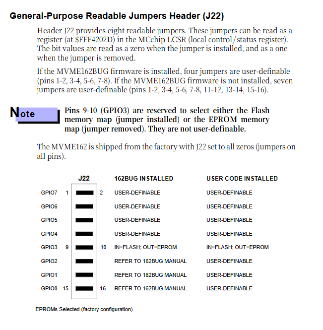
Jumper configuration: The board contains multiple configurable jumper caps, which are factory default configurations and can be modified according to needs. The core jumper functions are shown in the following table:
|Jumper number | Function | Factory configuration | Optional configuration|
|J1 | System Controller Selection | 1-2 Short Circuit (for VMEbus System Controller) | Remove Jumper (for Non System Controller)|
|J11 | Serial port 1/console clock | No jumper (asynchronous communication) | 1-2, 3-4 short circuit (synchronous external clock)|
|J12 | Serial port 2 clock | No jumper (asynchronous communication) | 1-2, 3-4 short circuit (synchronous external clock)|
|J20 | SRAM backup power supply | 1-3, 2-4 short circuit (VMEbus+5V backup power supply) | 3-5, 4-6 short circuit (onboard battery)|
|J21 | EPROM Capacity Selection | 2-3 Short Circuit (4Mbit, Only Available Specification) | -|
|J22 | Universal readable jumper | Fully short circuited (all 0) | Partially removed, corresponding register value is 1, GPO3 (9-10) is used to select Flash/EPROM|
SIM serial port module: Serial port 2 (Port B) is equipped with a SIM module through the J10 interface, supporting four types of DTE/DCE: EIA-232D/EIA-530. The module can be plugged and replaced, and the core model is SIM05-SIM08;
Module installation
IP modules: up to 4 can be installed, corresponding to J2/J3, J7/J8, J13/J14, J18/J19 interfaces, supporting dual size IP modules;
MVME162 board: If it is a system controller, it needs to be installed in slot 1 on the leftmost side of the VME chassis. The IACK/BG jumper in the slot needs to be removed and firmly connected to the P1/P2 backplane connector;
Transition module: MVME712 series transition module is required, only its serial ports 2/4 can be used, and 1/3 and printer ports are prohibited. This module cannot be used when configuring EIA-530;
System supporting requirements: To complete the MVME162 system setup, it is necessary to provide the system console terminal, disk drives and controllers, operating system, MVME712 transition module+P2/LCP2 adapter board and cables.
Operation instructions
This chapter introduces the front-end panel operations, memory mapping rules, software initialization, and reset operations of MVME162, which are the core basis for device use and program development
Front panel controls
Buttons: ABORT (S1) (Generate programmable interrupt after software enable, return 162Bug), RESET (S2) (Reset all devices on the board, if it is a system controller, drive SYSRESET *);
8 LED indicator lights: FAIL (red, BRDFAIL * activated), STAT (yellow, processor paused), RUN (green, local bus cycle executed), SCON (green, for VMEbus system controller), LAN (green, LAN chip is local bus master device), FUSE (green, LAN transceiver power is normal), SCSI (green, SCSI chip is local bus master device), VME (green, using VMEbus);
Memory mapping: divided into two types: local bus memory mapping and VMEbus memory mapping. The local bus address range is
00000000−
FFFFFFFF, The core partition includes programmable DRAM/SRAM/IP memory areas
FF800000−
FF9FFFFF's Flash/EPROM area
FFF00000−
FFFEFFFF's local I/O device area (including various registers)
FFFF0000−
VMEbus A16 area of FFFFFFFF; The local I/O device area includes core registers such as VMEchip2, MCchip, SCC, LAN, SCSI, IPIC, TOD clock, etc. The manual provides detailed definitions of the addresses, bit widths, and functions of each register;
BBRAM/TOD clock mapping: The 8KB NVRAM of MK48T08 is divided into user area, network area, system area, debugging area, configuration area (256B), TOD clock area (8B). The configuration area stores key information such as card serial number, Ethernet address, SCSI ID, etc., and the last byte is the checksum;
Software initialization: The 162Bug debugging firmware completes the default configuration of most control registers during power on/reset. If custom configuration is required, please refer to the M68040 manual and MVME162 programming reference guide; In a multi MPU system, only one MPU control register is allowed at a time to avoid conflicts;
Reset operation
System reset (SYSRESET *): triggered by the reset button, power on, watchdog timeout, and VMEchip2 LCSR bit, lasting at least 200ms and complying with the VMEbus specification;
Local Reset (LRST): a subset of system reset, with 5 triggering methods (watchdog timeout, reset key, GCSR bit, etc.) SYSRESET*、 Power on), the VMEbus master device can reset the local bus through GCSR, which carries risks and is only used in case of device failure.
Function module analysis
This chapter analyzes the working principles, interface specifications, and timing performance of each core module of MVME162 from the perspective of hardware architecture. The core content includes:
Local bus architecture: 32-bit synchronous bus, based on MC68040 bus, supports burst transmission and listening, bus arbitration is priority arbitration, and the priority of the main device from high to low is LAN (82596CA)>SCSI (53C710)>VMEbus>MPU;
Core storage module
DRAM: Controlled by MCchip, with programmable base address and capacity, parity errors can trigger interrupts/bus exceptions, requiring at least 10 initialization cycles;
SRAM: 512KB 32-bit, powered by Dallas DS1210S for battery backup, supporting dual backup of VMEbus+5V backup power supply and onboard battery. The onboard battery is RAYOVAC FB1225 (two BR1225 lithium batteries), which can be backed up for at least 2 years in a 40 ℃ power outage state;
Flash/EPROM: Bus conversion from 8-bit to 32-bit is implemented by MCchip, and reset code reading source (Flash/EPROM) is selected through GPIO of J22;
Communication and Expansion Interface
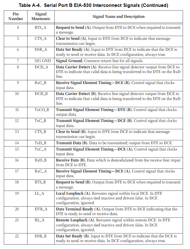
Dual serial ports: controlled by Zilog Z85230, serial port 1 is EIA-232-D DCE, and serial port 2 can be selected from EIA-232-D/EIA-530 DTE/DCE, supporting asynchronous (110B/s-38.4KB/s) and synchronous (SDLC/HDLC) protocols, and supporting CTS/DCD/RTS/DTR control signals;
Ethernet: controlled by Intel 82596CA, with 32-bit local bus DMA, the unique Ethernet address of the board is $08003E2xxxxx, stored on BBRAM and board labels, LAN DMA cannot access VMEbus to avoid buffer overflow;
SCSI: Controlled by NCR 53C710, with 32-bit local bus burst DMA, supports SCSI bus, and requires correct termination at both ends of the bus. The adapter board provides a termination resistor slot and fuse;
Industry Pack: Controlled by IPIC ASIC, supports 4 IP interfaces with 3M connectors, programmable memory/I/O space, and supports interrupt control;
VMEbus: Implemented by VMEchip2 ASIC, factory optional configuration, does not support on-site installation, supports A24/A32 addresses, D8/D16/D32 data, supports DMA burst transfer (D64/MBLT), provides system controller, interrupt handling, bus arbitration and other functions;
Local resources
Programmable timers: 4 MCchips+22 VMEchips, 32-bit, 1 μ s resolution, capable of generating periodic interrupts;
Watchdog timer: 1 each for MCchip and VMEchip2, working independently, timeout can trigger SYSRESET *, local reset, and board fault signals;
Hardware interrupts: VMEchip2 provides 8 software programmable hardware interrupts that can be triggered by software;
Local bus timeout: Both VMEchip2 and MCchip provide timeout function, with a timeout value of 8/64/256 μ s/infinite. After timeout, a TEA signal is sent to the main device. MCchip implements this function for boards without VMEbus;
Timing performance: The core is DRAM read and write cycles, with non interleaved DRAM read cycles of 4,2,2,2, interleaved DRAM read cycles of 4,1,1,1, and write cycles of 3,2,2 at 25MHz; EPROM/Flash cycle is 3-10 bus clock/byte, programmable configuration; The SCSI DMA transfer rate is 44MB/s (25MHz, no checksum, interleaved DRAM), and the LAN DMA transfer rate is 20MB/s (25MHz, no checksum).
Serial port interconnection specification
This chapter provides a detailed definition of the interconnection standard for MVME162 dual serial ports, supporting two specifications: EIA-232-D and EIA-530. The core content includes:
EIA-232-D: Single ended signal, DB25 interface, defined signal function for 25 pins, core uses TxD/RxD/RTS/CTS/DSR/DCD/DTR/SG, suitable for short distance transmission (recommended ≤ 15m), total load capacitance ≤ 2500pF, manual defines the electrical characteristics of transmitter/receiver (minimum output voltage ± 8.5V, input threshold ± 2.25V/± 0.75V);
EIA-530: Supports balanced/single ended signals, DB25 interface, upgraded to EIA-232-D, supports higher transmission rates, core signal is differential signal (such as TxD_A/TxD_B), manual defines the electrical characteristics of transmitter/receiver (differential output voltage ≥ 2.0V, input threshold ± 200mV);
Grounding requirements: The signal ground (Pin7) must be connected to complete the circuit loop; Use with caution the chassis ground (Pin1) to avoid current and data interference caused by different device ground potential differences. Only connect the signal ground to the chassis ground at one location (recommended on the computer side).
- YOKOGAWA
- Reliance
- ADVANCED
- SEW
- ProSoft
- WATLOW
- Kongsberg
- FANUC
- VSD
- DCS
- PLC
- man-machine
- Covid-19
- Energy and Gender
- Energy Access
- Renewable Integration
- Energy Subsidies
- Energy and Water
- Net zero emission
- Energy Security
- Critical Minerals
- A-B
- petroleum
- Mine scale
- Sewage treatment
- cement
- architecture
- Industrial information
- New energy
- Automobile market
- electricity
- Construction site
- HIMA
- ABB
- Rockwell
- Schneider Modicon
- Siemens
- xYCOM
- Yaskawa
- Woodward
- BOSCH Rexroth
- MOOG
- General Electric
- American NI
- Rolls-Royce
- CTI
- Honeywell
- EMERSON
- MAN
- GE
- TRICONEX
- Control Wave
- ALSTOM
- AMAT
- STUDER
- KONGSBERG
- MOTOROLA
- DANAHER MOTION
- Bentley
- Galil
- EATON
- MOLEX
- Triconex
- DEIF
- B&W
- ZYGO
- Aerotech
- DANFOSS
- KOLLMORGEN
- Beijer
- Endress+Hauser
- schneider
- Foxboro
- KB
- REXROTH
- YAMAHA
- Johnson
- Westinghouse
- WAGO
- TOSHIBA
- TEKTRONIX
- BENDER
- BMCM
- SMC
- HITACHI
- HIRSCHMANN
- XP POWER
- Baldor
- Meggitt
- SHINKAWA
- Other Brands
- UniOP
- KUKA
- IBA
- Beckhoff
- ADLINK
-
Beckhoff CP6500-1012-0060 - Control Cabinet PC Interface Unit
-
Beckhoff FC5202-0000 - 2-Channel DeviceNet Master PCI Interface Card
-
Beckhoff CP6606-0001-0020 - 7-Inch Economy Panel PC Touch
-
Beckhoff CP2921-0010 - Multi-Touch Integrated Control Panel Display
-
Beckhoff CP7802-0001-0010 - 15-Inch Touch Screen Control Panel HMI
-
Beckhoff C6920-0050 - Control Cabinet Industrial PC
-
Beckhoff BK9105 - EtherNet/IP Bus Coupler Network Interface
-
Beckhoff 31 Modules - Bus Terminal Slice I/O Lot Assortment
-
Beckhoff CX2020-0120 - Embedded PC Basic CPU Module 8GB CFast Card
-
Beckhoff CP7001-0000 - HMI Control Panel Touch Screen
-
B&R 7EX484.50-1 - System 2005 Controller Base Module Slots
-
Beckhoff EK1322 - 2-Port EtherCAT P Extension Feed-In Terminal
-
Beckhoff CP6606-0001-0020 - 7-Inch Single-Touch Economy Panel PC
-
Beckhoff CP6607-0001-0000 - Economy Installation Operator Panel PC 5.7-Inch
-
Beckhoff AX5103-0000-0200 - Digital Compact Servo Driver 3 Phase
-
Beckhoff CP7802-0001-0010 - 15-Inch Touch Screen Control Panel
-
Beckhoff AX8620 - Power Supply Module Axis System
-
Beckhoff CX2030-0121 - Embedded PC Controller Module
-
Beckhoff CP6606-0001-0020 - 7-Inch Economy Panel PC Touch Screen
-
Beckhoff CX2030-0121 - Embedded PC CPU Module Windows Standard 7
-
Beckhoff BX3100-0000 - PROFIBUS DP Bus Terminal Controller
-
Beckhoff CX1020-0000 - Controller Set with Power Supply Unit
-
Beckhoff EK1100 - EtherCAT Coupler Terminal Module Set
-
Beckhoff CP7002-1043-0010 - HMI Display Panel with Control Panel Bracket
-
Beckhoff AM8031-0D10-0000 - Synchronous Servo Motor
-
Beckhoff CX5130-0175 - Embedded PC 4GB RAM Controller
-
Beckhoff CX5130-0155 - Embedded PC Automation Controller
-
Beckhoff C6930-0010 - Control Cabinet Industrial PC Core Duo
-
Beckhoff CP3924-0000 - Multi-Touch Control Panel Display
-
Beckhoff AM8023-0F20-0000 - Synchronous Servo Motor
-
B&R KL3362 - Bus Terminal Thermocouple Input Module
-
Beckhoff AL2006-0000-0000 - Linear Servo Motor Three Phase
-
Beckhoff CX5140-0155 - Embedded PC CPU Controller Module
-
Beckhoff FC9002 - Ethernet PCI Network Interface Card
-
Beckhoff CP7203-0021-0040 - Built-In Panel PC 19-Inch Touch Screen
-
Beckhoff C6930-0020 - Control Cabinet Industrial PC HDD CF Card
-
Beckhoff CX2900-0033 - Memory Card CFast Storage
-
Beckhoff CP6201-0001-0020 - Built-In Panel PC Display
-
b+m surface systems C6930-1121-0060 - Industrial PC Beckhoff Core i7
-
Beckhoff CP2221-0010 - Multi-Touch Built-In Panel PC
-
Beckhoff C6017-0010 - Ultra-Compact Industrial PC
-
Beckhoff FC5102-0000 - 2-Channel CANopen PCI Interface Card
-
Beckhoff CP7021-0000-0000 - HMI Control Panel Interface
-
Beckhoff CP2216-0020 - Multi-Touch Built-In Panel PC
-
Beckhoff C6140 - Industrial PC Tower System Pentium 4
-
Beckhoff AM3033-1E40 - Servo Motor with Gearbox Assembly
-
Beckhoff CX9020-0115 - Embedded PC CPU Controller Module
-
Beckhoff CP6809-0001-0000 - Built-In Control Panel HMI Terminal
-
Beckhoff CP3919-0000 - Multi-Touch Control Panel Touchscreen Monitor
-
Beckhoff AM8053-0LHB-0000 - Synchronous Servo Motor
-
Beckhoff C6920-1028-0000 - Control Cabinet Industrial Computer PC
-
Beckhoff CX1100-0014 - Power Supply Unit for CX1030
-
Beckhoff CX9001-0101 - Embedded PC CPU Controller Module
-
Beckhoff CP3916-1428-0000 - Control Panel Multi-Touch Monitor
-
Beckhoff CP7037-1027-0010 - HMI Built-In Control Panel PC
-
Beckhoff CX1020-0120 - CPU Module DVI USB Windows Standard
-
Beckhoff CX5020-0121 - Embedded PC Controller Module
-
Beckhoff EL5042 - 2-Channel Encoder Interface BiSS C EtherCAT Terminal
-
Beckhoff CP7201-0021-0040 - Built-In Panel PC Touch Monitor
-
B&R X20-RT-8401 - reACTION Technology Module I/O Block
-
Beckhoff CP2915-0010 - HMI Control Panel Display Touch Screen
-
Beckhoff EL7221 - Servomotor Cyber Terminal EtherCAT Module
-
Beckhoff CX5140-0175 - Embedded PC CPU Module
-
Beckhoff C6017-0010 - Ultra-Compact Industrial PC
-
Beckhoff CX2020-0130 - Embedded PC Basic CPU Module
-
Beckhoff CX1030-0011 - Basic CPU Module Windows CE 6.0
-
Beckhoff AM8043-1E00-0000 - Synchronous Servo Motor
-
Beckhoff CX1020-0110 - CPU Module Controller Interface Bundle
-
Beckhoff C6930-1069-0030 - Control Cabinet Industrial PC Mainboard CB3054-0001
-
Beckhoff KL9528 - Power Supply Terminal Module
-
Beckhoff AM8053-0K20-0000 - Synchronous Servo Motor
-
Beckhoff CX5020-1111 - Embedded PC Controller Module
-
Beckhoff CX5130-0175 - Embedded PC CPU Module Intel Atom
-
Beckhoff CP6401-1024-0040 - Husky Display Control Panel HMI Terminal
-
Beckhoff CP2616-0000 - Multi-Touch Display Automation Panel PC
-
Beckhoff CP7921-1075-0000 - 12-Inch HMI Control Panel ELO Touch
-
Beckhoff C6930-0060 - Control Cabinet Industrial PC SSD
-
Beckhoff AX5112-0000 - Digital Compact Servo Drive 3 Phase
-
Beckhoff C6930-0040 - Control Cabinet Industrial PC Intel Core i5
-
Beckhoff CP2616-0000 - Multi-Touch Display Automation Panel PC
-
Beckhoff KL1414 - 4-Channel Digital Input Bus Terminal
-
Beckhoff CX1020-0000 - Basic CPU Module Controller
-
Beckhoff CP6201-1008-0000 - 12-Inch Built-In Panel PC
-
Beckhoff CP7021-0000 - HMI Control Panel Display Screen
-
Beckhoff AX5106-0000 - Digital Compact Servo Drive
-
Beckhoff BX3100-0000 - Profibus DP Bus Terminal Controller
-
Beckhoff CP2916-0000 - Multi-Touch Built-In Control Panel
-
Beckhoff C6925-0030 - Fanless Control Cabinet Industrial PC
-
Beckhoff C6330 - Industrial PC Motherboard Boser HS6237 Celeron
-
Beckhoff AM3033-0C00-0000 - Synchronous Servo Motor
-
Beckhoff CP7232-0001-0030 - Control Panel PC HMI
-
Beckhoff CX5020-0122 - Embedded PC CPU Module
-
Beckhoff AM8043-0H10-0000 - Rotary Synchronous Servo Motor
-
Beckhoff CP3924-0010 - Multitouch Control Panel HMI
-
Beckhoff CX9020-0110-1005 - Embedded PC Basic CPU Module
-
Beckhoff BK9105 - EtherNet/IP Bus Coupler
-
Beckhoff CX1500-M310 - Profibus Master Fieldbus Extension Module
-
Beckhoff CX1500-M510 - PROFIBUS Master Fieldbus Extension Module
-
Beckhoff CP9922.0 - TTL-TX Display Transmitter Card
-
Beckhoff CP9010_1 - ISA Slot Interface Card
-
Beckhoff NRL75-DC30S15B - LCD Inverter Board
-
Beckhoff LTD121C30S - Toshiba LCD Display Panel
-
Beckhoff CP7732-1207-0030 - Operating Terminal Panel PC HMI
-
Beckhoff C5102-0010 - Rackmount Industrial Computer PC5000
-
Beckhoff C6015-0010 - Ultra-Compact Industrial PC
-
Beckhoff CB1056-0001 - Industrial PC Motherboard Mainboard
-
Beckhoff AX5103 - Digital Compact Servo Amplifier 1 Axis
-
Beckhoff AM8052-0J00-9000 - Rotary Synchronous Servo Motor
-
Beckhoff CP7932-0002-0000 - Control Panel HMI Display
-
Beckhoff CB1061-0001 - Industrial PC Motherboard Mainboard
-
Beckhoff C5102-0060 - 19-inch Rackmount Industrial PC
-
Beckhoff EL7342 - 2 Channel DC Motor Motion Interface EtherCAT Terminal
-
Beckhoff CX5120-0135 - Embedded PC CPU Module Intel Atom
-
Beckhoff CB1061-G4 - Industrial PC Motherboard Mainboard
-
Beckhoff CX50100121 - Embedded PC CPU Module
-
Beckhoff CX1030-0013-1002 - Basic CPU Module Intel Pentium M
-
Beckhoff CP7802-1075-0010 - Control Panel Touch Screen HMI
-
Beckhoff AM8023-0E20-0000 - Rotary Synchronous Servo Motor
-
Beckhoff EL5032 - 2 Channel Encoder Interface EnDAT EtherCAT Terminal
-
Beckhoff CX5130-0175 - Embedded PC CPU Module Intel Atom
-
Beckhoff CA4040-0000 - PCI Ethernet Network Board
-
Beckhoff C3340 - Panel PC Industrial Workstation
-
Beckhoff EL3068 - 8 Channel Analog Input EtherCAT Terminal 0-10V
-
Beckhoff EL1889 - 16 Channel Digital Input EtherCAT Terminal
-
Beckhoff C6640-0050 - Control Cabinet Industrial PC Intel Core i7
-
Beckhoff PC MIC 3230 TP - Industrial Panel PC Touch Screen
-
Beckhoff CX2040-0135 - Embedded PC Industrial CPU Module
-
Beckhoff CP6202-1020-0010 - Built-in Panel PC HMI

K-JIANG

Add: Jimei North Road, Jimei District, Xiamen, Fujian, China
Tell:+86-15305925923