
K-WANG


GE VMIVME-3115-010 32-Channel 12-bit Analog Output Board
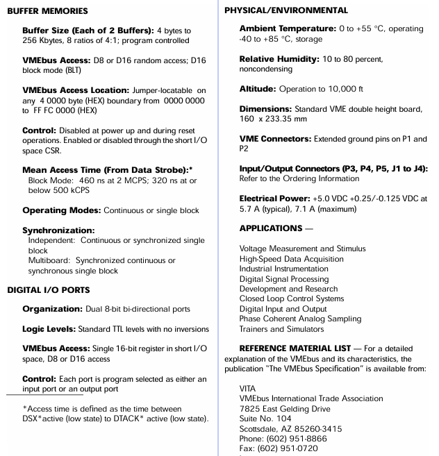
Dual-ported data memory, on-board timers, and a program-controlled bus interrupter enables the VMIVME-3115 board to support extensive analog input and output traffic with minimum involvement of the host processor.
GE VMIVME-3115-010 32-Channel 12-bit Analog Output Board
ANALOG INPUTS
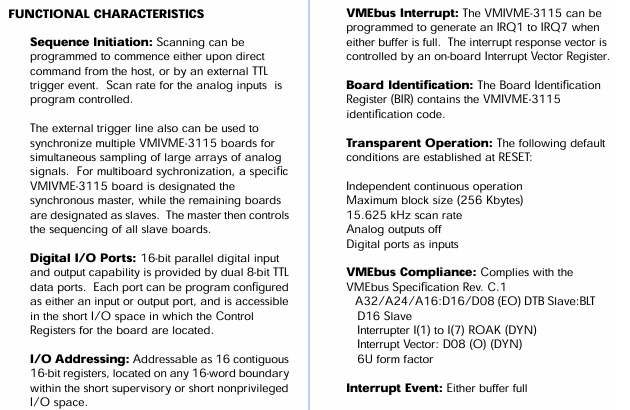
Dual-ported data memory, on-board timers, and a program-controlled bus interrupter enables the VMIVME-3115 board to support extensive analog input and output traffic with minimum involvement of the host processor.
Sample-and-hold input amplifiers provide “snapshot” simultaneous sampling of all analog inputs at aggregate sample rates up to 2 MHz, and virtually eliminate time skewing between input channels. The VMIVME-3115 supports both independent and multiboard synchronization. Dual analog outputs enable the board to “close the loop” in system servo applications.
memory to the VME host. Total memory space occupied by the board is 256 Kbytes, and can be program located on any 4 0000 byte (HEX) boundary in the VMEbus memory space. The VMIVME-3115 buffers can be removed (masked) from VMEbus memory by a CSR control bit.
I/O Address Selection: Board address in the short I/O space is selected by on-board field selectable jumpers.
Operation is supported in any slot except slot 1.
6U form factor
Interrupt Event: Either buffer full

- YOKOGAWA
- Reliance
- ADVANCED
- SEW
- ProSoft
- WATLOW
- Kongsberg
- FANUC
- VSD
- DCS
- PLC
- man-machine
- Covid-19
- Energy and Gender
- Energy Access
- Renewable Integration
- Energy Subsidies
- Energy and Water
- Net zero emission
- Energy Security
- Critical Minerals
- A-B
- petroleum
- Mine scale
- Sewage treatment
- cement
- architecture
- Industrial information
- New energy
- Automobile market
- electricity
- Construction site
- HIMA
- ABB
- Rockwell
- Schneider Modicon
- Siemens
- xYCOM
- Yaskawa
- Woodward
- BOSCH Rexroth
- MOOG
- General Electric
- American NI
- Rolls-Royce
- CTI
- Honeywell
- EMERSON
- MAN
- GE
- TRICONEX
- Control Wave
- ALSTOM
- AMAT
- STUDER
- KONGSBERG
- MOTOROLA
- DANAHER MOTION
- Bentley
- Galil
- EATON
- MOLEX
- Triconex
- DEIF
- B&W
- ZYGO
- Aerotech
- DANFOSS
- KOLLMORGEN
- Beijer
- Endress+Hauser
- schneider
- Foxboro
- KB
- REXROTH
- YAMAHA
- Johnson
- Westinghouse
- WAGO
- TOSHIBA
- TEKTRONIX
- BENDER
- BMCM
- SMC
- HITACHI
- HIRSCHMANN
- XP POWER
- Baldor
- Meggitt
- SHINKAWA
- Other Brands
- UniOP
- KUKA
- IBA
- Beckhoff
- ADLINK
-
Beckhoff EP9224-0037 - 4-Channel Power Distribution Box EtherCAT
-
Beckhoff CX2900-0026 - Solid State Flash Memory Card 20GB CFast
-
Beckhoff BK7500 - SERCOS Interface Fieldbus Bus Coupler Terminal
-
Beckhoff Ep2328-0002 - 4-Channel Input 4-Channel Output EtherCAT Box IP67
-
Beckhoff CX1020-0111 - Controller Kit Combo Interface Modules
-
B&R X20AI2237 - X20 System Analog Input Interface Module
-
Beckhoff CP2221-0010 - Multi-Touch Built-In Panel PC Touchscreen
-
Beckhoff CX1500-M310 - Fieldbus Master Interface Module 24V
-
Beckhoff CX2100-0904 - Power Charging Module Smart UPS Extension
-
Beckhoff CP3918-0000 - Multi-Touch Control Panel 18.5-Inch Monitor
-
Beckhoff CP2915-0000 - 15-Inch Multi-Touch Built-In Control Panel
-
Beckhoff CP7037-1027 - HMI Industrial Control Panel Built-In PC
-
Beckhoff EL3152 - 2-Channel Analog Input Terminal 4-20mA EtherCAT
-
Beckhoff CP6607-0000-0020 - 5.7-Inch Built-In Panel PC HMI Touch
-
Beckhoff EJ1809-0000 - 16-Channel Digital Input Pluggable Signal Level Terminal
-
Beckhoff AM8563-0N10-0000 - Synchronous Servo Motor
-
Beckhoff AX2006-S60600-520 - Compact Servo Drive Inverter
-
Beckhoff AM8053-0K20-0000 - Servo Motor with Planetary Gearbox AG3210
-
Beckhoff AM8042-0FH1-0000 - Synchronous Servo Motor
-
Rexroth R911338600 - IndraControl V HMI Terminal Beckhoff PCI Card FC9002
-
Beckhoff AX5125-0000 - 3 Phase Industrial Servo Drive 1000Hz
-
Beckhoff EP2328-0002 - 4-Channel Digital Input 4-Channel Output EtherCAT Box
-
B&R 7CP476-02 - System 2005 RTD CPU Module 3IF681.86 Interface
-
Beckhoff AX8620-0000-0000 - Power Supply Module Axis Drive System
-
Beckhoff CX1010-0111 - PLC Module CPU Controller 24V
-
Beckhoff AM8043-0H10-0000 - Synchronous Servo Motor
-
Beckhoff C6240-1009 - Control Cabinet Industrial PC Mainframe
-
Beckhoff BX8000-0000 - Bus Terminal Controller HW 4.4 Standalone
-
Beckhoff CP7721-1089-0020 - 12.1-Inch Touch Screen HMI Panel PC
-
Beckhoff CP7132-0001 - Industrial Built-In Panel PC Screen
-
Beckhoff CP2912-0010 - Multi-Touch Built-In Control Panel Display
-
Beckhoff CP2915-0000 - 15-Inch Multi-Touch Built-In Control Panel
-
Beckhoff AM8532-1EN0-0000 - Synchronous Servo Motor
-
Beckhoff AX5203-0000 - 2-Channel Digital Compact Servo Drive
-
Beckhoff CX2020-0141 - Embedded PC Core CPU Module
-
Beckhoff CP6832-0002-0010 - Built-In Industrial Control Panel Display
-
Beckhoff CX5020-0112 - Embedded PC CPU Control Module
-
Beckhoff CX5140-0175 - 4GB Embedded PC CPU Unit 24V
-
Beckhoff EL3681-0030 - Digital Multimeter Calibration Terminal EtherCAT
-
Beckhoff CP7201-1000-0000 - Industrial PC Touch Screen HMI Monitor
-
Beckhoff CP7232-1001-0000 - Industrial Panel PC Touch Screen
-
Beckhoff C6930-1032-0040 - Control Cabinet Industrial PC System
-
Beckhoff AX5125-0000 - 3 Phase Industrial Servo Drive 1000Hz
-
Beckhoff CP3916-1424-0000 - Multi-Touch Built-In Control Panel
-
B&R 1900071142 - Lemoine Fieldbus Communication Interface Module
-
Beckhoff EL2872 - 16-Channel Ribbon Cable Digital Output Terminal
-
Beckhoff CX2030-0120 - Embedded PC CPU Base Module Controller
-
Beckhoff CP3919-0000 - 19-Inch Multi-Touch Control Panel Touchscreen
-
Beckhoff AX5101-0000-0202 - Servo Driver Compact Intelligent Drive 180V
-
Beckhoff CX5130-0135 - Embedded PC Controller Module
-
Beckhoff CP3719-1061-0010 - Multi-Touch Panel PC Outer Housing Enclosure
-
Beckhoff CP3919-1033-0000 - 19-Inch Touch Industrial Panel Keyboard
-
Beckhoff CX5020-0111 - Embedded PC PLC CPU Module
-
Beckhoff FC5102-0000 - 2-Channel CANopen PCI Control Board Card
-
Beckhoff CX9001-1101 - Embedded PC CPU Network I/O System Module
-
Beckhoff CX1100-0920 - Smart Position Sensor Interface Module
-
B&R 4P3040.01-490 - Operator Panel PLC Interface Communication Module
-
Beckhoff CP2612-0000 - Dual-Touch Built-In Panel PC HMI
-
Beckhoff CP7002-1043-0010 - Touchscreen Display HMI Panel Terminal
-
Beckhoff CX9020-0115 - Embedded PC Controller Module
-
Beckhoff CX5140-0155 - 4GB Embedded PC CPU Module Die Industry
-
B&R 7DI435.7 - System 2005 Universal Digital Input Output Module
-
Bihl+Wiedemann BWU1568 - AS-i Master to Profibus Gateway Module
-
Beckhoff C6920-0070 - Control Cabinet Industrial PC 8GB Win 10
-
B&R X20AI2322 - 2-Channel Temperature Analog Input Module
-
Beckhoff CP2912-0000 - 12-Inch Touchscreen Display Monitor Screen
-
Beckhoff CP6022-1001-0010 - 15-Inch Built-In Control Panel
-
Beckhoff AM8031-0D10-0000 - Synchronous Servo Motor
-
Beckhoff CX5010-0111 - Embedded PC Controller CPU Module
-
Beckhoff CP7232-1000-0000 - Industrial Panel PC Touch Display Screen
-
Beckhoff CP7802-0011-0000 - 15-Inch Industrial Touchscreen Control Panel
-
Beckhoff C6320 - Control Cabinet Industrial PC
-
Beckhoff CX1030-0012 - Basic CPU Module Windows CE 6.0
-
Beckhoff CP2919-0000 - Installation Multi-Touch Control Panel
-
Beckhoff CX1020-0000 - Controller Set Stack System Pack
-
B&R 3DO480.6 - System 2005 Digital Output Module
-
Beckhoff EL3101 - 1-Channel Analog Input Terminal Differential +/-10V
-
Beckhoff AX8108-0200-0000 - Axis Feed Module Servo Drive
-
Beckhoff CP7802-1241-0010 - 15-Inch Industrial Touchscreen Control Panel
-
Beckhoff FC2002-0000 - 2-Channel Lightbus Data Acquisition PCI Card
-
Beckhoff CX5120-0155 - 2GB Embedded PC Intel Atom Controller
-
Beckhoff Cx9020-0111 - 1GB Basic CPU Module Embedded PC
-
Beckhoff CP6901-0001-0000 - 12-Inch Economy Built-In Control Panel
-
Beckhoff CX9020-0111 - Embedded PC CPU Basic Module
-
Beckhoff CX5130-0100 - 4GB Embedded PC CPU Module
-
Beckhoff CP2715-0010 - Multi-Touch Built-In Panel PC
-
Beckhoff CX2033-0175 - Embedded PC CPU Module Core i7
-
Beckhoff CP7201-1000-0000 - 12-Inch Touchscreen Panel PC AMAT Green Box
-
Beckhoff EL4038 - 8-Channel Analog Output Terminal 0-10V EtherCAT
-
Beckhoff CP6802-0000-0000 - Built-In Control Panel HMI Screen
-
Beckhoff CP6500-1012-0060 - Control Cabinet PC Interface Unit
-
Beckhoff FC5202-0000 - 2-Channel DeviceNet Master PCI Interface Card
-
Beckhoff CP6606-0001-0020 - 7-Inch Economy Panel PC Touch
-
Beckhoff CP2921-0010 - Multi-Touch Integrated Control Panel Display
-
Beckhoff CP7802-0001-0010 - 15-Inch Touch Screen Control Panel HMI
-
Beckhoff C6920-0050 - Control Cabinet Industrial PC
-
Beckhoff BK9105 - EtherNet/IP Bus Coupler Network Interface
-
Beckhoff 31 Modules - Bus Terminal Slice I/O Lot Assortment
-
Beckhoff CX2020-0120 - Embedded PC Basic CPU Module 8GB CFast Card
-
Beckhoff CP7001-0000 - HMI Control Panel Touch Screen
-
B&R 7EX484.50-1 - System 2005 Controller Base Module Slots
-
Beckhoff EK1322 - 2-Port EtherCAT P Extension Feed-In Terminal
-
Beckhoff CP6606-0001-0020 - 7-Inch Single-Touch Economy Panel PC
-
Beckhoff CP6607-0001-0000 - Economy Installation Operator Panel PC 5.7-Inch
-
Beckhoff AX5103-0000-0200 - Digital Compact Servo Driver 3 Phase
-
Beckhoff CP7802-0001-0010 - 15-Inch Touch Screen Control Panel
-
Beckhoff AX8620 - Power Supply Module Axis System
-
Beckhoff CX2030-0121 - Embedded PC Controller Module
-
Beckhoff CP6606-0001-0020 - 7-Inch Economy Panel PC Touch Screen
-
Beckhoff CX2030-0121 - Embedded PC CPU Module Windows Standard 7
-
Beckhoff BX3100-0000 - PROFIBUS DP Bus Terminal Controller
-
Beckhoff CX1020-0000 - Controller Set with Power Supply Unit
-
Beckhoff EK1100 - EtherCAT Coupler Terminal Module Set
-
Beckhoff CP7002-1043-0010 - HMI Display Panel with Control Panel Bracket
-
Beckhoff AM8031-0D10-0000 - Synchronous Servo Motor
-
Beckhoff CX5130-0175 - Embedded PC 4GB RAM Controller
-
Beckhoff CX5130-0155 - Embedded PC Automation Controller
-
Beckhoff C6930-0010 - Control Cabinet Industrial PC Core Duo
-
Beckhoff CP3924-0000 - Multi-Touch Control Panel Display
-
Beckhoff AM8023-0F20-0000 - Synchronous Servo Motor
-
B&R KL3362 - Bus Terminal Thermocouple Input Module
-
Beckhoff AL2006-0000-0000 - Linear Servo Motor Three Phase
-
Beckhoff CX5140-0155 - Embedded PC CPU Controller Module
-
Beckhoff FC9002 - Ethernet PCI Network Interface Card
-
Beckhoff CP7203-0021-0040 - Built-In Panel PC 19-Inch Touch Screen
-
Beckhoff C6930-0020 - Control Cabinet Industrial PC HDD CF Card
-
Beckhoff CX2900-0033 - Memory Card CFast Storage
-
Beckhoff CP6201-0001-0020 - Built-In Panel PC Display

K-JIANG

Add: Jimei North Road, Jimei District, Xiamen, Fujian, China
Tell:+86-15305925923