
K-WANG


GE VMIVME-3125 Analog Input Board
GE VMIVME-3125 Analog Input Board
Product Overview
VMIVME-3125 is a flexible and low-cost analog input board that adopts the VMEbus 6U single height format and provides 16 differential or 32 single ended analog input channels. The channels are digitized using a 12 bit resolution analog-to-digital converter (ADC). This board does not require software settings, and will automatically start scanning all input channels after power on or system reset. The converted data is stored in dual port memory and can be accessed immediately through VMEbus. It also has a built-in self-test (BIT) function, and the input voltage range and gain can be programmed by the user through jumper wires. The VMEbus base address and access mode can be fully selected.
Core Features
16 differential or 32 single ended analog input channels.
1 12 bit A/D converter with built-in tracking and holding function.
All inputs are automatically scanned at a total rate of 40 kHz.
Scanning can begin without software initialization.
The input range is from ± 50 mV to ± 10 VDC.
Input overvoltage protection, analog input is low-pass filtered at 50 kHz, and an optional 40 Hz low-pass filter sub board can be added.
Supports discrete or large-scale terminated cables.
Input pull-down resistor to prevent input floating.
Supports both online and offline built-in testing (BIT).
The programmable gain of the jumper is x1, x10, x100.
The optional A/D range is ± 5 VDC, ± 10 VDC, and 0 to 10 VDC.
Data access methods: D16, D08 (EO), D08 (O).
Front panel LED indicator light.
1000 VDC isolation between analog ground and digital ground.
Optional 0-20, 4-20, and 5-25 mA current input ranges.
Working principle
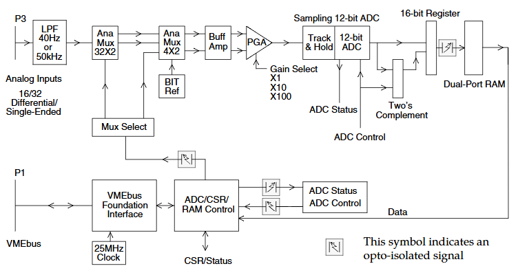
Functional components: mainly including VMEbus interface, analog-to-digital converter (ADC) and control logic, analog input multiplexing, gain and conversion, BIT voltage reference and multiplexer, board ID register and other functional parts.
VMEbus interface: Communication registers are mapped to 64 16 bit words (128 bytes) in memory, which can be located on any 128 byte boundary within the VMEbus short I/O space and can be configured to respond to short monitoring or short non privileged data access.
Analog to digital conversion control and timing: There are two operating modes, namely continuous scanning of all 16 or 32 analog input channels, and stopping scanning and locking to a single channel. Using a 12 bit ADC with a conversion time of 8.5 μ sec, the channel acquisition cycle is once every 25 μ sec, and the total scanning rate is 40 kHz. The ADC's built-in tracking and holding device can prevent erroneous readings from signals that change during the conversion cycle.
Built in Test Reference: Equipped with programmable precision voltage reference for board built-in testing (BIT). When selected, the BIT voltage is fed to the ADC through a programmable gain amplifier, bypassing the external analog input on channel 0. Users can enable BIT during initial board installation or real-time system self diagnosis.
Analog Input: The front panel connector provides 16 differential or 32 single ended analog inputs. It is recommended to use differential mode to reduce noise and improve common mode rejection ratio. Unused inputs should be grounded, and the low end of the differential input on the board has an internal 22 M Ω pull-down resistor.
Low pass filter: Provides a passive single pole low-pass input filter with a normal -3 dB cut-off frequency of 50 kHz, and can also be configured with an additional sub board to provide a low-pass filter with a cut-off frequency of 40 Hz.
Input multiplexer: There are two levels of analog multiplexing, with each of the 32 inputs selected through one of the four 8x1 first level analog input multiplexers. The second level multiplexer is configured as a 4x2 board, and one or two of the first level output signals are selected to provide single ended or differential operation mode. BIT reference voltage can also be selected.
Programmable gain instrumentation amplifier: After selecting the input channel and passing through the input multiplexer, it enters the programmable gain amplifier as a differential input. The differential amplifier suppresses common mode noise and delivers the scaled single ended output to the ADC. The hardware can jumper the gain to 1, 10, and 100.
Channel sequencer and dual port RAM memory: typically run in scan mode, starting conversion immediately after power on or reset. After A/D conversion is completed, the dual port control logic retrieves the conversion data and stores it in the corresponding dual port register of the channel. The channel counter increments and selects the next channel to be multiplexed to the ADC. After all input channels are converted and stored, the channel counter resets and starts the channel scanning sequence again. The channel sequencer can be stopped at the current address by the stop auto scan bit in the control/status register.
Board ID Register: The first position of the VMIVME-3125 register group is the read-only board ID register, with a value of $37, used for general system software to automatically determine the installed board.
Built in power converter and ADC power supply: The power supply for the analog circuit is provided by an onboard DC-DC converter, which converts the+5 VDC of VMEbus to a regulated ± 15 VDC. The+5 VDC logic power supply for the ADC is provided by an onboard regulator, and a separate+5 V DC-DC converter is used to provide isolated analog ground for the ADC.
Configuration and Installation
Unpacking procedure: Components may be sensitive to electrostatic discharge. When handling, the board should be placed on conductive material. After unpacking, check for any transportation damage. If there is any damage, file a claim with the carrier and report to GE.
Physical installation: Power off installation, insert the board into the appropriate slot of the chassis, ensure correct alignment and orientation, smoothly slide towards the mating connector until firmly seated.
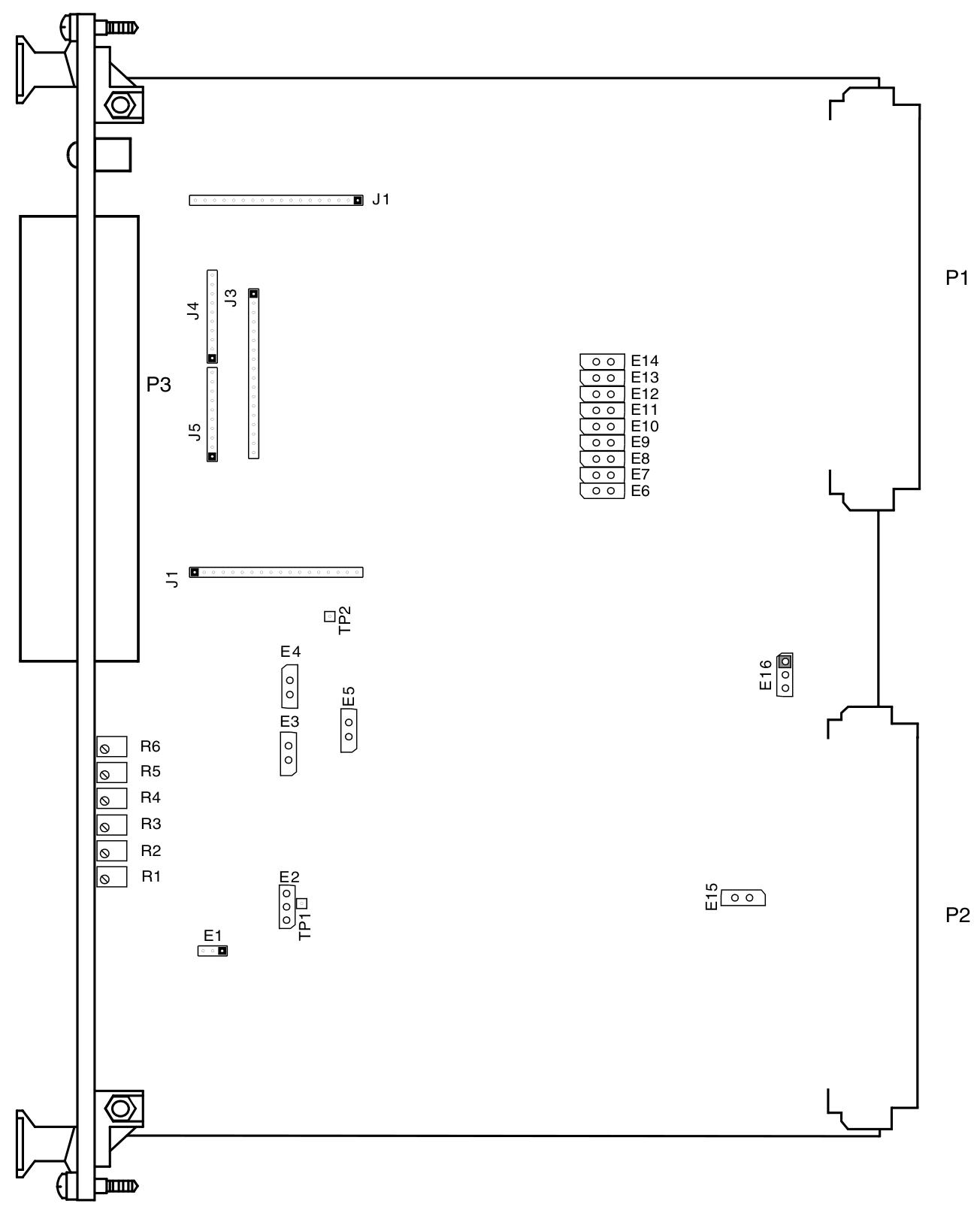
Jumper installation
Board address: occupies a short I/O address space of 128 consecutive bytes, with the base address controlled by jumper E6 to E14. The installed jumper corresponds to binary 0, and the uninstalled one corresponds to binary 1. The factory default address is short I/O $0000 (all jumper installations).
Address modifier: Jumper E16 determines the access mode of the response, including monitoring, non privileged, or both.
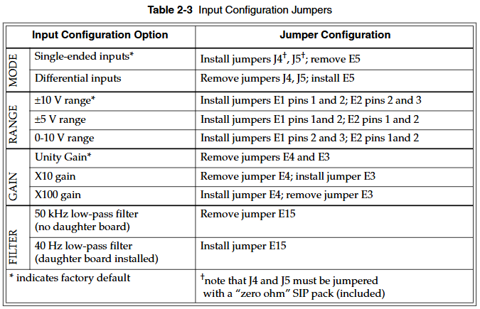
Input configuration: Three jumpers (J4, J5, and E5) are used to configure single ended or differential inputs, two jumpers (E1 and E2) control the input voltage range, two jumpers (E3 and E4) control the gain, and there are filter related jumpers. The factory default configuration is single ended, ± 10 V range, and unity gain.
Analog input connector description: 16 differential or 32 single ended analog input connections are made through the front panel 37 pin D-type connector P3, with corresponding pins and signal allocation.
Calibration Procedure: To obtain the specified accuracy of analog measurements, calibration is required for the required range and input topology. Firstly, instrument amplifier offset and BIT voltage calibration are performed, and then the corresponding offset and gain calibration procedures for the input topology are selected. Calibration requires a 5-digit digital voltmeter (DVM) and precision voltage reference equipment.
Programming
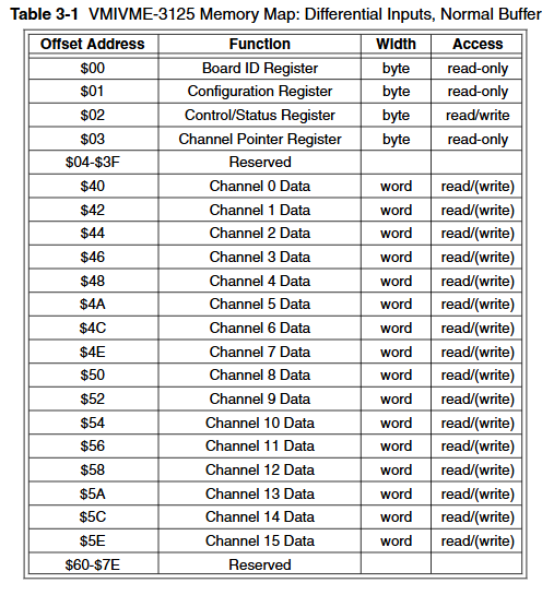
Memory mapping: occupying 128 bytes of address space, including four information and control registers, as well as a conversion data register. Depending on the jumper configuration of the board (single ended or differential input, normal or maximum buffer for differential input), there are different memory mapping tables.
Register description
Board ID register: 8-bit read-only register, offset $00, value $37, used to uniquely identify the board.
Configuration register: 8-bit read-only register, offset $01, indicating the current configuration, including input mode and filter bandwidth information.
Control/Status Register: 8-bit read/write register with an offset of $02, allowing software to control the board and indicate its current status, including functions such as stopping automatic scanning, maximum buffer, complement, mode bit, LED off, etc.
Channel pointer register: an 8-bit read-only register with an offset of $03, typically storing the input channel number currently being sampled and converted. Under specific configurations, it can determine the most recently updated data register.
Data registers: Depending on the state of the maximum buffer location, there are 16 or 32 data registers. Starting from an offset of $40, each 12 bit conversion data containing its related channel is aligned to the right within the 16 bit data register.
Built in testing function: It can test the function by applying various internal reference voltages to channel 0 input. The host software can read the value of channel 0 and compare it with the expected value. There are corresponding BIT value tables for different ranges and gain settings.
Range and gain determination: The analog gain and range can be set by the user, but the software cannot directly read these settings. It is not recommended to determine the current settings through BIT voltage stimulation, as the board must be calibrated to a single gain and range setting.
Accessing data in byte form: Data registers should typically be accessed using a single 16 bit word transfer, or two consecutive byte transfers, but there is a risk of confusion caused by data updates, which can be avoided by pausing automatic scanning or ensuring that byte accesses are continuous and undisturbed.
Current input options: VMIVME-3125-200 and VMIVME-3125-300 offer different terminal resistances, and the ADC input voltage is related to the current range, allowing for the calculation of the current signal through a formula.
- YOKOGAWA
- Reliance
- ADVANCED
- SEW
- ProSoft
- WATLOW
- Kongsberg
- FANUC
- VSD
- DCS
- PLC
- man-machine
- Covid-19
- Energy and Gender
- Energy Access
- Renewable Integration
- Energy Subsidies
- Energy and Water
- Net zero emission
- Energy Security
- Critical Minerals
- A-B
- petroleum
- Mine scale
- Sewage treatment
- cement
- architecture
- Industrial information
- New energy
- Automobile market
- electricity
- Construction site
- HIMA
- ABB
- Rockwell
- Schneider Modicon
- Siemens
- xYCOM
- Yaskawa
- Woodward
- BOSCH Rexroth
- MOOG
- General Electric
- American NI
- Rolls-Royce
- CTI
- Honeywell
- EMERSON
- MAN
- GE
- TRICONEX
- Control Wave
- ALSTOM
- AMAT
- STUDER
- KONGSBERG
- MOTOROLA
- DANAHER MOTION
- Bentley
- Galil
- EATON
- MOLEX
- Triconex
- DEIF
- B&W
- ZYGO
- Aerotech
- DANFOSS
- KOLLMORGEN
- Beijer
- Endress+Hauser
- schneider
- Foxboro
- KB
- REXROTH
- YAMAHA
- Johnson
- Westinghouse
- WAGO
- TOSHIBA
- TEKTRONIX
- BENDER
- BMCM
- SMC
- HITACHI
- HIRSCHMANN
- XP POWER
- Baldor
- Meggitt
- SHINKAWA
- Other Brands
- UniOP
- KUKA
- IBA
- Beckhoff
-
ADLINK PCI-7433 - switch value acquisition card Isolated Digital Input Card
-
ADLINK PCI-9112 - 51-12252-0D20 Multi-Function Data Acquisition Card
-
ADLINK NUPRO-A301 REV:1.4 - industrial control motherboard PICMG Full-Size SBC
-
ADLINK 51-18502-0A10 - Frame Grabber Image Acquisition Interface Card
-
ADLINK PCI-7296 - 51-12009-0A50 PCB-I-E-925=6DX1 96-CH Parallel Digital I/O Board
-
ADLINK PCI-8132 GP A2 - Motion Control Card 2-Axis Servo & Stepper Controller
-
ADLINK PCI-7442 - switch quantity card data acquisition card 64-CH Isolated Card
-
ADLINK HPX-13S4 - baseboard PICMG 1.3 Passive Backplane Chassis Baseplate
-
ADLINK NuPRO-590 / NTC-567-ZM-F36 - Single Board Computer PCB-I-E-1853=9L21 Half-Size SBC
-
ADLINK PCIe-8332 - 16-axis plate Motion Control Hardware Card
-
ADLINK NuPRO-775 REV.B1 - motherboard Pentium 4 Full-Size PICMG SBC
-
ADLINK PXI-3920 - Embedded Controller 3U PXI cPCI System Intelligence Board
-
ADLINK PCI-8134 - driver card motion control card 4-Axis Controller Board
-
ADLINK HSL-DI32-M-N-011 / HSL-TB32-M-DIN - Digital Input & Base Module PLC Distributed I/O System
-
ADLINK PCI-6216V-206 / PCI-208V 009 - 16 CH 16bit analog output card
-
ADLINK NuPro-E330 - 51-41805-0A20 PCB Single Board Computer Host Board
-
ADLINK PCI-1622C - Card 8-Port RS-232/422/485 PCI Serial Communication Board
-
ADLINK PCIe-7432 - 51-18402-0A10 Carte PCIe Avec Plage D'Entrée Élevée Isolated DIO Card
-
ADLINK PCI-7250 - PCI Acquisition Card 8-CH Relay Output Isolated DI Card
-
ADLINK PCI-7230 - 32-CH Isolated Digital I/O Card
-
ADLINK PCI-8164 - PCB 4-Axis Motion Controller Card
-
ADLINK PCI-7854 - Collection card High-Speed Link Distributed Motion Controller
-
ADLINK NuPRO-935A/LV - industrial control computer motherboard Full-Size PICMG SBC
-
ADLINK IMB-M40H - motherboard IH61-AA4 1155 LGA1155 Micro-ATX Mainboard
-
ADLINK PCI-7248 - Linhua 51-12006-0A40 48-CH Parallel Digital I/O Card
-
ADLINK HPCI-14S12U - Linhua industrial computer baseboard Passive Backplane
-
ADLINK PCI-8132 Rev.A2 - 2-Axis Servo & Stepper Motion Controller Card
-
ADLINK ACL-8111 - ISA card Multi-Function DAQ Card
-
ADLINK ACL-8111 - ISA card Multi-Function Data Acquisition Board
-
ADLINK PCI-7200 REV.A3 - Digital I/O card 12MB/s High-Speed Parallel Digital I/O
-
ADLINK PCI-7296 REV.A3 - 96-CH High-Density Opto-Isolated DIO Card
-
ADLINK PCI-7434 - 64-CH Isolated Digital Output Card
-
ADLINK M-342 - atx motherboard Industrial PC Mainboard
-
ADLINK NuPRO-935ADV (A) 1.9 - CPU Board Intel Core 2 Quad CPU Q9500 2.83GHz PICMG Board
-
ADLINK NUPRO-935A/DV - motherboard dual network port 51-41802-0A10 CPU Board
-
ADLINK PCI-RTV24 - image capture card Analog Video Frame Grabber Board
-
ADLINK HPX-13S4 - device baseboard PICMG 1.3 Passive Backplane Chassis Baseplate
-
ADLINK PCI-8134A - control card 4-Axis Motion Controller Card
-
ADLINK ACL-7130 REV. B2 - industrial control capture card Isolated Digital I/O Board
-
ADLINK EBP-13E2 - Industrial Backplane Board Passive Backplane Baseboard
-
ADLINK NuPRO-935ADV (A) 1.9 - CPU Board Intel Core 2 Quad CPU Q9500 2.83GHz PICMG SBC
-
ADLINK PCI-8134A - motion control card 4-Axis Pulse-Train Controller Card
-
ADLINK PCI-9112 REV A.1 - Multi Function DA&C Board Data Acquisition Card
-
ADLINK 51-12001-0C20 - Circuit Board Multi-Function Data Acquisition Hardware
-
ADLINK PCI-7300A - 80-CH High-Speed Digital I/O Card
-
ADLINK PCI-7230 - 16-CH Isolated Digital Input Output Card
-
ADLINK DIN-814-GP - motion control module Interface Terminal Block
-
ADLINK NUPRO-A40H - 51-41807-1A20 Industrial Control Motherboard LGA1155
-
ADLINK PCI-7433 rev A2 - Isolated Digital Input Card
-
ADLINK NuPRO-780 - Pentium III 800 512 MB SBC NuPRO780 51-41309-0B2 Single Board Computer
-
ADLINK PCI-7853 / PCI-7854 - Acquisition card High-Speed Link Control Card
-
ADLINK NUPRO-852 / NUPRO-852LV - Industrial motherboard Full-Size PICMG CPU Board
-
ADLINK NuPRO-842LV/P - 51-41360-0B30 Industrial Motherboard Half-Size PICMG SBC
-
ADLINK PCI-FIW64 - 4/2 Channel IEEE1394B Image Capture Card Frame Grabber
-
ADLINK PCI-7851 Rev A1.1 - HSL system card High-Speed Link Master Controller
-
ADLINK PCI-7230 - 51-12003-0A50 card 32-CH Isolated Digital I/O Card
-
ADLINK NuPRO-841REV:1.0 - Industrial CPU Board Mainboard
-
ADLINK NuPRO-841 REV:1.0 - motherboard Industrial Control PC Mainboard
-
ADLINK PCI-8256 - 8-Axis Advanced Motion Control PCI Board
-
ADLINK PCI-6S / PCI6S - Backplane 6-Slot Passive Backplane Board
-
ADLINK PCI-7234 REV B3 - 32-CH Isolated Digital Output PCI Card
-
ADLINK PCI-8213 - HannStar MV-4 51-45003-0b4 Board
-
ADLINK PCI-7233 - 51-12004-0a20 board PCI7233 32-CH Isolated Digital Input Card
-
ADLINK PCI-7851 - 006 51-24003-0B20 High-Speed Link Master Motion Control Card
-
ADLINK PCI-7432 - 64-CH Isolated Digital I/O PCI Cards
-
ADLINK LPCI-3488 - Card Low Profile IEEE-488 GPIB Interface Card
-
ADLINK HPCI14S REV.B1 - industrial control computer base plate Passive Backplane
-
ADLINK NEON-1020 - Industrial camera Smart Camera Vision System
-
ADLINK PCI-7432 - Isolated Digital I/O PCI Card 64-CH
-
ADLINK Pcm-7250+ - 8-Ch Relay Outputs & 8-Ch Isolated DI Module PC/104
-
ADLINK CPCI-7841 - DUAL-PORT ISOLATED CAN INTERFACE CARD CompactPCI
-
ADLINK PCI-3488 / PCI-GPIB - PCI IEEE-488 GPIB Interface Card
-
ADLINK PCI-1711U - Card Multi-Function Data Acquisition Board
-
ADLINK NUPRO-A301 - REV:1.1 1.2 1.4 PICMG Full-Size Single Board Computer
-
Adlink DIN-50S-01 - PLOTECH 51-14024-0A40 50-pin Wiring Terminal Board
-
Chroma 52962 / 58183 - PXI Optical Spectrometer carrier adapter Card
-
ADLINK PCI-6208V - PCI DATA ACQUISITION & RECORDING CARD 8-CH Analog Output
-
ADLINK HSL-DI32-DB-N - Industrial Control Board Distributed Digital Input Module
-
ADLINK HSL-AO4-U - 4-CH HIGH SPEED LINK ANALOG OUTPUT MODULE Distributed I/O
-
ADLINK PCI-7396 - 0050 GP 51-12012-0B20 96-CH High-Speed Digital I/O Card
-
ADLINK NUPRO-935A/DV - 51-41802-0A10 motherboard Industrial CPU Single Board Computer
-
ADLINK PCI-9111 DG - Industrial Acquisition Card Multi-Function DAQ Card
-
ADLINK NuPRO-E315 - industrial computer motherboard Intel Atom SHB SBC
-
ADLINK NUPRO-406 REV:B1 - Industrial Control Motherboard Full-Size PICMG CPU Board
-
ADLINK NuPRO-E330 - motherboard Industrial Control System Host Board PICMG 1.3
-
ADLINK ACL-6128A 103 - 51-11002-1A4 2-CH Isolated Analog Output Card
-
XTRAMUS cPS-H325/AC - POWER SUPPLY NUSTREAMS 600 NETWORK TESTING EQUIPMENT Power Module
-
ADLINK DIN-814P-A4 - 51-14056-0A10 Terminal Block Motion Control Breakout Board
-
ADLINK TB-24P/24-01 - 24-Channel Card Terminal Breakout Board
-
ADLINK PCI-7251 - 51-12008-0A30 PCI7251 8-CH Relay Output Isolated Digital Input Card
-
ADLINK HSL-TB64-DIN REV A1 / HSL-DO32-DB-N - 2ea Board Breakout Terminal Board Distributed I/O Module
-
ADLINK NuPRO-865 REV 3.0 - industrial computer motherboard Full-Size PICMG SBC
-
ADLINK NUPRO-A40H - motherboard 51-41807-1A30 OSP H61 Industrial PC Mainboard
-
ADLINK LPCI-3488A - PCI Card 51-12801-0A30 GPIB Interface Card
-
ADLINK DIN-825-4P0 - 51-14085-0A30 Terminal Printed Circuit Board Breakout Block
-
ADLINK IMB-T10/D2550 V - MOTHER BOARD 80-PXG160-A1A01 IMB-T10-M2G-S32G Industrial Mainboard
-
ADLINK PCI-8144N - Motion Control card Stepper Motor Controller
-
ADLINK PCI-7433 - Digital acquisition card Isolated Digital Input Card
-
ADLINK PCI-9112 DG - Data Acquisition card 51-12252-0D20 Multi-Function DAQ
-
ADLINK IMB-M40H - motherboard IH61-AA4 1155 LGA1155 Micro-ATX Mainboard
-
ADLINK TB-24P/24-01 - Carte 24 voies Terminal Breakout Board Connector Module
-
ADLINK HSL-D16DO16-M-NN - Distributed Discrete Input Output I/O Module
-
ADLINK PCI-7248 - PCI CARD 51-12006-0A40 48-CH Parallel Digital I/O Board
-
ADLINK HSL-DI32-DB-N - Industrial Control Board Distributed I/O Digital Input Module
-
ADLINK PCI-7433 - Pci 7433 Isolated Digital Input Card
-
ADLINK PCI-6208V - 008 Data acquisition card 8-CH Analog Output Card
-
ADLINK IH61-AA4 - industrial motherboard LGA1155 Micro-ATX Mainboard
-
ADLINK PXI-3920 - PXI 3U cPCI Industrial Controller Embedded System CPU Board
-
ADLINK PCI-6308 - Analog Output DAQ Card Isolated Voltage Output Card
-
ADLINK PCI-7200 - data acquisition card REV.A3 High-Speed Parallel DIO Card
-
ADLINK NuPRO-E315 - Industrial Control Computer Motherboard PICMG 1.3 SHB SBC
-
ADLINK PCI-1610C - Card 4-Port Isolated RS-232 PCI Serial Communication Card
-
ADLINK PCI-1716 - Card High-Resolution Multi-Function DAQ Card
-
ADLINK MI-965 - Industrial Mini-ITX Motherboard CPU Board
-
ADLINK PCI-1610A - Card 4-Port RS-232 PCI Serial Communication Card
-
ADLINK cBP-3208/3208R - CPCI Board 3U 8-Slot CompactPCI Backplane
-
ADLINK PCI-8134A - 51-12421-0A10 4-Axis Motion Controller Card
-
ADLINK PCI-8164 - Motion Control Card 4-Axis Advanced Controller Card
-
ADLINK NUPRO-935A/DV - motherboard dual network port 51-41802-0A10 CPU Board
-
ADLINK PCI-7248 - 51-12006-0A40 acquisition card 48-CH Parallel DIO Card
-
ADLINK PCI-7443 - 51-12022-0A10 BOARD 128-CH Isolated Digital Input Card
-
ADLINK DIN-825-GP4 - Terminal Block Interface Board Breakout Module
-
ADLINK PCI-7248 - Card 48-CH Parallel Digital I/O Card
-
ADLINK NUPRO-865 REV :3.0 - industrial motherboard Intel Pentium 4 CPU Board
-
ADLINK PCI-9113A - Isolated Analog Input Data Acquisition Card
-
ADLINK HPCI-8S4 - REV.B2 Industrial Control Base Plate Passive Backplane
-
ADLINK M-342 - atx motherboard Industrial PC Mainboard
-
ADLINK PCI-RTV24 - image capture card Analog Video Frame Grabber Board

K-JIANG

Add: Jimei North Road, Jimei District, Xiamen, Fujian, China
Tell:+86-15305925923