
K-WANG
+086-15305925923
Service expert in industrial control field!


Product
Article
NameDescriptionContent
Adequate Inventory, Timely Service
pursuit of excellence


Ship control system
Equipment control system
Power monitoring system
Current position:
新闻动态
newS
Brand
GE VMIVME-5565 Ultrahigh-Speed Fiber-Optic Reflective Memory with Interrupts
GE VMIVME-5565 Ultrahigh-Speed Fiber-Optic Reflective Memory with Interrupts
GE VMIVME-5565 Ultrahigh-Speed Fiber-Optic Reflective Memory with Interrupts
The VMIVME-7807/VME-7807RC provide a programmable Watchdog Timer (WDT)
which can be used to reset the system if software integrity fails.
WDT Control Status Register (WCSR)
The WDT is controlled and monitored by the WDT Control Status Register (WCSR)
which is located at offset 0x08 from the address in BAR2. The mapping of the bits in
this register are as follows:
The “WDT Timeout Select” field is used to select the timeout value of the Watchdog
Timer as follows:
The “SERR/RST Select” bit is used to select whether the WDT generates an SERR# on
the local PCI bus or a system reset. If this bit is set to “0”, the WDT will generate a
system reset. Otherwise, the WDT will make the local PCI bus SERR# signal active.
The “WDT Enable” bit is used to enable the Watchdog Timer function. This bit must
be set to “1” in order for the Watchdog Timer to function. Note that since all registers
default to zero after reset, the Watchdog Timer is always disabled after a reset. The
Watchdog Timer must be re-enabled by the application software after reset in order
for the Watchdog Timer to continue to operate. Once the Watchdog Timer is enabled,
the application software must refresh the Watchdog Timer within the selected timeout
period to prevent a reset or SERR# from being generated. The Watchdog Timer is
Field Bits Read or Write
SERR/RST Select WCSR[16] R/W
WDT Timeout Select WCSR[10..8] R/W
WDT Enable WCSR[0] R/W
All of these bits default to “0” after system reset. All other bits are reserved.
Timeout WCSR[10] WCSR[9] WCSR[8]
135s 0 0 0
33.6s 0 0 1
2.1s 0 1 0
524ms 0 1 1
262ms 1 0 0
131ms 1 0 1
32.768ms 1 1 0
2.048ms 1 1 1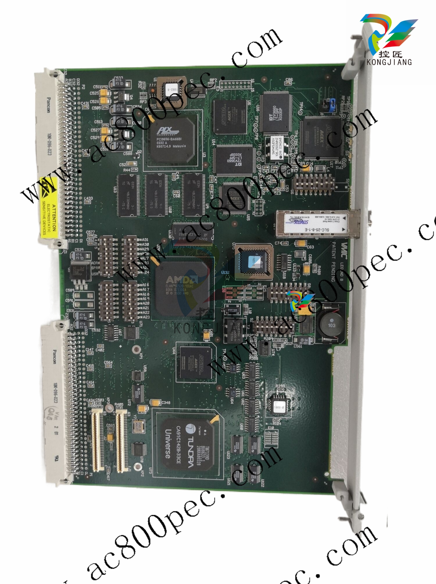
The following table shows the register definitions for the VMIVME-7807/
VME-7807RC (offset from BAR0).
Please refer to Table 3-1, “PCI Configuration Space Registers,” on page 47 for more
information concerning BAR0.
Table 3-2 Register Definitions Offset From BAR0
Register Name Offset
VMECOMM 0x00
Bit Name Bit Definition
MEC_SEL 0 Master big-endian enable bit 1=Big Endian,
0=Little Endian bit
SEC_SEL 1 Slave Big-Endian enable bit 1=Big Endian,
0=Little Endian
ABLE 2 Auxiliary BERR logic enable bit
1=Aux. BERR enabled 0=Aux. BERR disabled
BTO 3 Bus error timer enabled 1=enabled, 0=disabled
BTOV [1:0] 5:4 Timeout value
00 - 16μs
01 - 64μs
10 -256μs
11 - 1.00ms
BERRI 6 BERR interrupt enable 1=Interrupt enabled
0=Interrupt disabled
BERRST 7 BERR status read/clear bit
1=Clear BERR status, 0=Do nothing
SFENA 8 Enables generation of VME SYSFAIL upon
WDT timeout
1= Enable SYSFAIL generation, 0=Disable
Unused 9 Not Used
BPENA 10 Endian conversion bypass bit
1=bypass, 0=Not bypassed
VBENA 11 VME enable bit (VBENA)
1 = enabled, 0 = disabled
Unused 31:12 Not Used
VBAM 0x04
VME_ADDR 5:0 Latched VME Address Modifier
Unused 31:6 Not Used
SEC_SEL 0x001
VBAR 0x08
VME_ADDR All Latched VME Address
- YOKOGAWA
- Reliance
- ADVANCED
- SEW
- ProSoft
- WATLOW
- Kongsberg
- FANUC
- VSD
- DCS
- PLC
- man-machine
- Covid-19
- Energy and Gender
- Energy Access
- Renewable Integration
- Energy Subsidies
- Energy and Water
- Net zero emission
- Energy Security
- Critical Minerals
- A-B
- petroleum
- Mine scale
- Sewage treatment
- cement
- architecture
- Industrial information
- New energy
- Automobile market
- electricity
- Construction site
- HIMA
- ABB
- Rockwell
- Schneider Modicon
- Siemens
- xYCOM
- Yaskawa
- Woodward
- BOSCH Rexroth
- MOOG
- General Electric
- American NI
- Rolls-Royce
- CTI
- Honeywell
- EMERSON
- MAN
- GE
- TRICONEX
- Control Wave
- ALSTOM
- AMAT
- STUDER
- KONGSBERG
- MOTOROLA
- DANAHER MOTION
- Bentley
- Galil
- EATON
- MOLEX
- Triconex
- DEIF
- B&W
- ZYGO
- Aerotech
- DANFOSS
- KOLLMORGEN
- Beijer
- Endress+Hauser
- schneider
- Foxboro
- KB
- REXROTH
- YAMAHA
- Johnson
- Westinghouse
- WAGO
- TOSHIBA
- TEKTRONIX
- BENDER
- BMCM
- SMC
- HITACHI
- HIRSCHMANN
- XP POWER
- Baldor
- Meggitt
- SHINKAWA
- Other Brands
- UniOP
- KUKA
- IBA
- Beckhoff
91
-
ADLINK PCI-7433 - switch value acquisition card Isolated Digital Input Card
-
ADLINK PCI-9112 - 51-12252-0D20 Multi-Function Data Acquisition Card
-
ADLINK NUPRO-A301 REV:1.4 - industrial control motherboard PICMG Full-Size SBC
-
ADLINK 51-18502-0A10 - Frame Grabber Image Acquisition Interface Card
-
ADLINK PCI-7296 - 51-12009-0A50 PCB-I-E-925=6DX1 96-CH Parallel Digital I/O Board
-
ADLINK PCI-8132 GP A2 - Motion Control Card 2-Axis Servo & Stepper Controller
-
ADLINK PCI-7442 - switch quantity card data acquisition card 64-CH Isolated Card
-
ADLINK HPX-13S4 - baseboard PICMG 1.3 Passive Backplane Chassis Baseplate
-
ADLINK NuPRO-590 / NTC-567-ZM-F36 - Single Board Computer PCB-I-E-1853=9L21 Half-Size SBC
-
ADLINK PCIe-8332 - 16-axis plate Motion Control Hardware Card
-
ADLINK NuPRO-775 REV.B1 - motherboard Pentium 4 Full-Size PICMG SBC
-
ADLINK PXI-3920 - Embedded Controller 3U PXI cPCI System Intelligence Board
-
ADLINK PCI-8134 - driver card motion control card 4-Axis Controller Board
-
ADLINK HSL-DI32-M-N-011 / HSL-TB32-M-DIN - Digital Input & Base Module PLC Distributed I/O System
-
ADLINK PCI-6216V-206 / PCI-208V 009 - 16 CH 16bit analog output card
-
ADLINK NuPro-E330 - 51-41805-0A20 PCB Single Board Computer Host Board
-
ADLINK PCI-1622C - Card 8-Port RS-232/422/485 PCI Serial Communication Board
-
ADLINK PCIe-7432 - 51-18402-0A10 Carte PCIe Avec Plage D'Entrée Élevée Isolated DIO Card
-
ADLINK PCI-7250 - PCI Acquisition Card 8-CH Relay Output Isolated DI Card
-
ADLINK PCI-7230 - 32-CH Isolated Digital I/O Card
-
ADLINK PCI-8164 - PCB 4-Axis Motion Controller Card
-
ADLINK PCI-7854 - Collection card High-Speed Link Distributed Motion Controller
-
ADLINK NuPRO-935A/LV - industrial control computer motherboard Full-Size PICMG SBC
-
ADLINK IMB-M40H - motherboard IH61-AA4 1155 LGA1155 Micro-ATX Mainboard
-
ADLINK PCI-7248 - Linhua 51-12006-0A40 48-CH Parallel Digital I/O Card
-
ADLINK HPCI-14S12U - Linhua industrial computer baseboard Passive Backplane
-
ADLINK PCI-8132 Rev.A2 - 2-Axis Servo & Stepper Motion Controller Card
-
ADLINK ACL-8111 - ISA card Multi-Function DAQ Card
-
ADLINK ACL-8111 - ISA card Multi-Function Data Acquisition Board
-
ADLINK PCI-7200 REV.A3 - Digital I/O card 12MB/s High-Speed Parallel Digital I/O
-
ADLINK PCI-7296 REV.A3 - 96-CH High-Density Opto-Isolated DIO Card
-
ADLINK PCI-7434 - 64-CH Isolated Digital Output Card
-
ADLINK M-342 - atx motherboard Industrial PC Mainboard
-
ADLINK NuPRO-935ADV (A) 1.9 - CPU Board Intel Core 2 Quad CPU Q9500 2.83GHz PICMG Board
-
ADLINK NUPRO-935A/DV - motherboard dual network port 51-41802-0A10 CPU Board
-
ADLINK PCI-RTV24 - image capture card Analog Video Frame Grabber Board
-
ADLINK HPX-13S4 - device baseboard PICMG 1.3 Passive Backplane Chassis Baseplate
-
ADLINK PCI-8134A - control card 4-Axis Motion Controller Card
-
ADLINK ACL-7130 REV. B2 - industrial control capture card Isolated Digital I/O Board
-
ADLINK EBP-13E2 - Industrial Backplane Board Passive Backplane Baseboard
-
ADLINK NuPRO-935ADV (A) 1.9 - CPU Board Intel Core 2 Quad CPU Q9500 2.83GHz PICMG SBC
-
ADLINK PCI-8134A - motion control card 4-Axis Pulse-Train Controller Card
-
ADLINK PCI-9112 REV A.1 - Multi Function DA&C Board Data Acquisition Card
-
ADLINK 51-12001-0C20 - Circuit Board Multi-Function Data Acquisition Hardware
-
ADLINK PCI-7300A - 80-CH High-Speed Digital I/O Card
-
ADLINK PCI-7230 - 16-CH Isolated Digital Input Output Card
-
ADLINK DIN-814-GP - motion control module Interface Terminal Block
-
ADLINK NUPRO-A40H - 51-41807-1A20 Industrial Control Motherboard LGA1155
-
ADLINK PCI-7433 rev A2 - Isolated Digital Input Card
-
ADLINK NuPRO-780 - Pentium III 800 512 MB SBC NuPRO780 51-41309-0B2 Single Board Computer
-
ADLINK PCI-7853 / PCI-7854 - Acquisition card High-Speed Link Control Card
-
ADLINK NUPRO-852 / NUPRO-852LV - Industrial motherboard Full-Size PICMG CPU Board
-
ADLINK NuPRO-842LV/P - 51-41360-0B30 Industrial Motherboard Half-Size PICMG SBC
-
ADLINK PCI-FIW64 - 4/2 Channel IEEE1394B Image Capture Card Frame Grabber
-
ADLINK PCI-7851 Rev A1.1 - HSL system card High-Speed Link Master Controller
-
ADLINK PCI-7230 - 51-12003-0A50 card 32-CH Isolated Digital I/O Card
-
ADLINK NuPRO-841REV:1.0 - Industrial CPU Board Mainboard
-
ADLINK NuPRO-841 REV:1.0 - motherboard Industrial Control PC Mainboard
-
ADLINK PCI-8256 - 8-Axis Advanced Motion Control PCI Board
-
ADLINK PCI-6S / PCI6S - Backplane 6-Slot Passive Backplane Board
-
ADLINK PCI-7234 REV B3 - 32-CH Isolated Digital Output PCI Card
-
ADLINK PCI-8213 - HannStar MV-4 51-45003-0b4 Board
-
ADLINK PCI-7233 - 51-12004-0a20 board PCI7233 32-CH Isolated Digital Input Card
-
ADLINK PCI-7851 - 006 51-24003-0B20 High-Speed Link Master Motion Control Card
-
ADLINK PCI-7432 - 64-CH Isolated Digital I/O PCI Cards
-
ADLINK LPCI-3488 - Card Low Profile IEEE-488 GPIB Interface Card
-
ADLINK HPCI14S REV.B1 - industrial control computer base plate Passive Backplane
-
ADLINK NEON-1020 - Industrial camera Smart Camera Vision System
-
ADLINK PCI-7432 - Isolated Digital I/O PCI Card 64-CH
-
ADLINK Pcm-7250+ - 8-Ch Relay Outputs & 8-Ch Isolated DI Module PC/104
-
ADLINK CPCI-7841 - DUAL-PORT ISOLATED CAN INTERFACE CARD CompactPCI
-
ADLINK PCI-3488 / PCI-GPIB - PCI IEEE-488 GPIB Interface Card
-
ADLINK PCI-1711U - Card Multi-Function Data Acquisition Board
-
ADLINK NUPRO-A301 - REV:1.1 1.2 1.4 PICMG Full-Size Single Board Computer
-
Adlink DIN-50S-01 - PLOTECH 51-14024-0A40 50-pin Wiring Terminal Board
-
Chroma 52962 / 58183 - PXI Optical Spectrometer carrier adapter Card
-
ADLINK PCI-6208V - PCI DATA ACQUISITION & RECORDING CARD 8-CH Analog Output
-
ADLINK HSL-DI32-DB-N - Industrial Control Board Distributed Digital Input Module
-
ADLINK HSL-AO4-U - 4-CH HIGH SPEED LINK ANALOG OUTPUT MODULE Distributed I/O
-
ADLINK PCI-7396 - 0050 GP 51-12012-0B20 96-CH High-Speed Digital I/O Card
-
ADLINK NUPRO-935A/DV - 51-41802-0A10 motherboard Industrial CPU Single Board Computer
-
ADLINK PCI-9111 DG - Industrial Acquisition Card Multi-Function DAQ Card
-
ADLINK NuPRO-E315 - industrial computer motherboard Intel Atom SHB SBC
-
ADLINK NUPRO-406 REV:B1 - Industrial Control Motherboard Full-Size PICMG CPU Board
-
ADLINK NuPRO-E330 - motherboard Industrial Control System Host Board PICMG 1.3
-
ADLINK ACL-6128A 103 - 51-11002-1A4 2-CH Isolated Analog Output Card
-
XTRAMUS cPS-H325/AC - POWER SUPPLY NUSTREAMS 600 NETWORK TESTING EQUIPMENT Power Module
-
ADLINK DIN-814P-A4 - 51-14056-0A10 Terminal Block Motion Control Breakout Board
-
ADLINK TB-24P/24-01 - 24-Channel Card Terminal Breakout Board
-
ADLINK PCI-7251 - 51-12008-0A30 PCI7251 8-CH Relay Output Isolated Digital Input Card
-
ADLINK HSL-TB64-DIN REV A1 / HSL-DO32-DB-N - 2ea Board Breakout Terminal Board Distributed I/O Module
-
ADLINK NuPRO-865 REV 3.0 - industrial computer motherboard Full-Size PICMG SBC
-
ADLINK NUPRO-A40H - motherboard 51-41807-1A30 OSP H61 Industrial PC Mainboard
-
ADLINK LPCI-3488A - PCI Card 51-12801-0A30 GPIB Interface Card
-
ADLINK DIN-825-4P0 - 51-14085-0A30 Terminal Printed Circuit Board Breakout Block
-
ADLINK IMB-T10/D2550 V - MOTHER BOARD 80-PXG160-A1A01 IMB-T10-M2G-S32G Industrial Mainboard
-
ADLINK PCI-8144N - Motion Control card Stepper Motor Controller
-
ADLINK PCI-7433 - Digital acquisition card Isolated Digital Input Card
-
ADLINK PCI-9112 DG - Data Acquisition card 51-12252-0D20 Multi-Function DAQ
-
ADLINK IMB-M40H - motherboard IH61-AA4 1155 LGA1155 Micro-ATX Mainboard
-
ADLINK TB-24P/24-01 - Carte 24 voies Terminal Breakout Board Connector Module
-
ADLINK HSL-D16DO16-M-NN - Distributed Discrete Input Output I/O Module
-
ADLINK PCI-7248 - PCI CARD 51-12006-0A40 48-CH Parallel Digital I/O Board
-
ADLINK HSL-DI32-DB-N - Industrial Control Board Distributed I/O Digital Input Module
-
ADLINK PCI-7433 - Pci 7433 Isolated Digital Input Card
-
ADLINK PCI-6208V - 008 Data acquisition card 8-CH Analog Output Card
-
ADLINK IH61-AA4 - industrial motherboard LGA1155 Micro-ATX Mainboard
-
ADLINK PXI-3920 - PXI 3U cPCI Industrial Controller Embedded System CPU Board
-
ADLINK PCI-6308 - Analog Output DAQ Card Isolated Voltage Output Card
-
ADLINK PCI-7200 - data acquisition card REV.A3 High-Speed Parallel DIO Card
-
ADLINK NuPRO-E315 - Industrial Control Computer Motherboard PICMG 1.3 SHB SBC
-
ADLINK PCI-1610C - Card 4-Port Isolated RS-232 PCI Serial Communication Card
-
ADLINK PCI-1716 - Card High-Resolution Multi-Function DAQ Card
-
ADLINK MI-965 - Industrial Mini-ITX Motherboard CPU Board
-
ADLINK PCI-1610A - Card 4-Port RS-232 PCI Serial Communication Card
-
ADLINK cBP-3208/3208R - CPCI Board 3U 8-Slot CompactPCI Backplane
-
ADLINK PCI-8134A - 51-12421-0A10 4-Axis Motion Controller Card
-
ADLINK PCI-8164 - Motion Control Card 4-Axis Advanced Controller Card
-
ADLINK NUPRO-935A/DV - motherboard dual network port 51-41802-0A10 CPU Board
-
ADLINK PCI-7248 - 51-12006-0A40 acquisition card 48-CH Parallel DIO Card
-
ADLINK PCI-7443 - 51-12022-0A10 BOARD 128-CH Isolated Digital Input Card
-
ADLINK DIN-825-GP4 - Terminal Block Interface Board Breakout Module
-
ADLINK PCI-7248 - Card 48-CH Parallel Digital I/O Card
-
ADLINK NUPRO-865 REV :3.0 - industrial motherboard Intel Pentium 4 CPU Board
-
ADLINK PCI-9113A - Isolated Analog Input Data Acquisition Card
-
ADLINK HPCI-8S4 - REV.B2 Industrial Control Base Plate Passive Backplane
-
ADLINK M-342 - atx motherboard Industrial PC Mainboard
-
ADLINK PCI-RTV24 - image capture card Analog Video Frame Grabber Board

K-JIANG

Add: Jimei North Road, Jimei District, Xiamen, Fujian, China
Tell:+86-15305925923