
K-WANG


AMAT 0040-54755 Ceramic ESC Semiconductor
Research on the Application of AMAT 0040-54755 Ceramic Electrostatic Suction Disk (ESC) in Semiconductor Manufacturing
1、 Introduction
In modern semiconductor manufacturing, equipment precision and processing stability are the core driving forces behind technological progress. Especially in the wafer processing, the wafer needs to be accurately and firmly fixed on the processing platform to achieve precise etching, deposition, cleaning, and measurement processes. Electrostatic Chuck (ESC), as an efficient and safe wafer fixing device, is gradually replacing traditional mechanical fixtures and becoming an indispensable component in modern semiconductor equipment.
AMAT 0040-54755 is a high-end ceramic electrostatic suction cup launched by Applied Materials (AMAT) in the United States, widely used in key processes such as plasma etching, PVD, CVD, ALD, etc. Its high reliability, excellent thermal uniformity, and outstanding electrical performance make it stand out among advanced process nodes.
This article will systematically analyze the product structure, functional principles, application scenarios, manufacturing processes, and market trends of AMAT 0040-54755.
2、 Basic principle of electrostatic suction cup
1. Working principle
The core principle of an electrostatic suction cup is based on electrostatic mechanical effects, and its basic structure includes: electrode layer, insulating ceramic layer, heating layer, back cooling system, etc. ESC typically forms an electrostatic field between the electrode and the wafer by applying a direct current or high-frequency voltage to the electrode, thereby adsorbing the wafer.
According to the different structures of the electrodes, ESC can be divided into two categories:
Monopolar ESC: Suitable for conductive wafers, with a simple structure.
Bipolar ESC: Suitable for non-conductive wafers, it generates electrostatic adsorption through two opposing electrodes.
2. Advantages of ceramic materials
AMAT 0040-54755 ESC uses high-purity alumina or aluminum nitride ceramics, and its main advantages include:
Strong insulation: Ensure electrical isolation between the electrode and the external environment to avoid the risk of leakage.
High thermal conductivity: helps maintain uniformity in wafer heating or cooling.
Good corrosion resistance: able to withstand plasma and corrosive gas environments.
Good thermal stability: suitable for high-temperature plasma treatment.
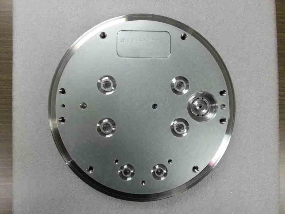
3、 AMAT 0040-54755 ESC Product Structure and Features
1. Product Structure
The typical structure of this ESC product is as follows:
Top ceramic panel: In direct contact with the wafer, it has good thermal conductivity and electrical insulation.
Electrode layer: embedded in ceramics, responsible for generating electrostatic forces.
Heating layer (optional): used to control wafer temperature, usually a thin film heater.
Cooling system: Maintain heat exchange between the wafer and the suction cup through helium back pressure.
Vacuum channels and positioning pin holes: assist in precise positioning of wafers and circulation of process gases.
2. Technical parameters (example)
Parameter values
Material: Aluminum Nitride/Aluminum Oxide Ceramic
Compatible with 300mm wafer size
Electrode type: Bipolar ESC
Working voltage 0~1000V DC
Working temperature from room temperature to 350 ° C
Vacuum adaptation supports high vacuum and plasma chamber environments
Back pressure control helium channel system (He Backside Pressure)
4、 The role of AMAT ESC in semiconductor processes
1. Plasma Etching
During the etching process, the wafer needs to be fixed in the reaction chamber to undergo high-energy plasma treatment. ESC provides a non mechanical adsorption method that avoids contamination and damage caused by fixtures while maintaining high stability. The ceramic material of AMAT 0040-54755 ESC has high resistance and corrosion resistance, making it particularly suitable for long-term operation in fluorine based plasma.
2. PVD and CVD
In physical vapor deposition (PVD) and chemical vapor deposition (CVD), ESC requires precise control of wafer temperature to ensure thickness uniformity and adhesion of thin film deposition. The high thermal conductivity of ceramic ESC enables it to quickly respond to temperature control systems.
3. ALD (Atomic Layer Deposition)
The ALD process requires extremely high temperature uniformity and process stability. AMAT's ceramic ESC ensures minimal temperature fluctuations on the wafer surface, thereby improving the uniformity and reliability of the film.
5、 Manufacturing and Quality Control Process
1. Ceramic molding process
The manufacturing of ceramic ESC begins with the formation of ceramic bodies, mainly through hot pressing sintering (HP) and isostatic pressing sintering (CIP), supplemented by high-temperature sintering furnace treatment.
2. Electrode embedding
By using laser processing or screen printing to embed electrodes inside ceramics, and then encapsulating them through multi-layer stacking technology, the electrodes can ensure long-term stable operation.
3. Vacuum sealing and testing
After the whole machine is assembled, it is ensured that there are no hidden dangers such as gas leaks or internal cracks through helium leak detection, X-ray inspection, and other methods.
4. Temperature uniformity test
Use an infrared thermal imager to detect the uniformity of surface heating on ESC, with a control error within ± 2 ° C.
6、 AMAT's technological advantages and market position
As a leading global semiconductor equipment supplier, AMAT has accumulated decades of research and development experience in the ESC field, and its ESC products have the following advantages:
Highly customizable capability: can provide personalized design based on the customer's cavity structure.
High reliability: The average lifespan of the product can reach more than 5 years, and it is suitable for various corrosive environments.
Complete service network: There are maintenance and technical support centers worldwide.
In the global ESC market, AMAT competes with manufacturers such as SHINKU, TOTO, and II-VI Maruwa, and its advantages in high-end equipment and advanced process nodes are particularly evident.
7、 Market prospects and technological trends of ESC
1. Market growth drivers
The development of advanced processes such as 3nm and 2nm places higher demands on the thermal stability and temperature control accuracy of ESC.
3D NAND, HPC, and AI chip manufacturing require more complex multi-layer etching processes.
The process of new materials such as GaN and SiC is gradually maturing, and the demand for compatibility of adsorption devices is increasing.
It is expected that by 2030, the global ESC market size will reach over 2 billion US dollars, with a compound annual growth rate of over 10%.
2. Direction of technological evolution
Double sided heating ESC: supports more complex temperature control strategies.
Intelligent ESC: Embedded with temperature, voltage, and pressure sensors to achieve self-monitoring and feedback regulation.
Low particle design: using plasma cleaning and other methods to improve surface cleanliness and reduce particle pollution.
- YOKOGAWA
- Reliance
- ADVANCED
- SEW
- ProSoft
- WATLOW
- Kongsberg
- FANUC
- VSD
- DCS
- PLC
- man-machine
- Covid-19
- Energy and Gender
- Energy Access
- Renewable Integration
- Energy Subsidies
- Energy and Water
- Net zero emission
- Energy Security
- Critical Minerals
- A-B
- petroleum
- Mine scale
- Sewage treatment
- cement
- architecture
- Industrial information
- New energy
- Automobile market
- electricity
- Construction site
- HIMA
- ABB
- Rockwell
- Schneider Modicon
- Siemens
- xYCOM
- Yaskawa
- Woodward
- BOSCH Rexroth
- MOOG
- General Electric
- American NI
- Rolls-Royce
- CTI
- Honeywell
- EMERSON
- MAN
- GE
- TRICONEX
- Control Wave
- ALSTOM
- AMAT
- STUDER
- KONGSBERG
- MOTOROLA
- DANAHER MOTION
- Bentley
- Galil
- EATON
- MOLEX
- Triconex
- DEIF
- B&W
- ZYGO
- Aerotech
- DANFOSS
- KOLLMORGEN
- Beijer
- Endress+Hauser
- schneider
- Foxboro
- KB
- REXROTH
- YAMAHA
- Johnson
- Westinghouse
- WAGO
- TOSHIBA
- TEKTRONIX
- BENDER
- BMCM
- SMC
- HITACHI
- HIRSCHMANN
- XP POWER
- Baldor
- Meggitt
- SHINKAWA
- Other Brands
- UniOP
- KUKA
- IBA
- Beckhoff
- ADLINK
-
Beckhoff EP9224-0037 - 4-Channel Power Distribution Box EtherCAT
-
Beckhoff CX2900-0026 - Solid State Flash Memory Card 20GB CFast
-
Beckhoff BK7500 - SERCOS Interface Fieldbus Bus Coupler Terminal
-
Beckhoff Ep2328-0002 - 4-Channel Input 4-Channel Output EtherCAT Box IP67
-
Beckhoff CX1020-0111 - Controller Kit Combo Interface Modules
-
B&R X20AI2237 - X20 System Analog Input Interface Module
-
Beckhoff CP2221-0010 - Multi-Touch Built-In Panel PC Touchscreen
-
Beckhoff CX1500-M310 - Fieldbus Master Interface Module 24V
-
Beckhoff CX2100-0904 - Power Charging Module Smart UPS Extension
-
Beckhoff CP3918-0000 - Multi-Touch Control Panel 18.5-Inch Monitor
-
Beckhoff CP2915-0000 - 15-Inch Multi-Touch Built-In Control Panel
-
Beckhoff CP7037-1027 - HMI Industrial Control Panel Built-In PC
-
Beckhoff EL3152 - 2-Channel Analog Input Terminal 4-20mA EtherCAT
-
Beckhoff CP6607-0000-0020 - 5.7-Inch Built-In Panel PC HMI Touch
-
Beckhoff EJ1809-0000 - 16-Channel Digital Input Pluggable Signal Level Terminal
-
Beckhoff AM8563-0N10-0000 - Synchronous Servo Motor
-
Beckhoff AX2006-S60600-520 - Compact Servo Drive Inverter
-
Beckhoff AM8053-0K20-0000 - Servo Motor with Planetary Gearbox AG3210
-
Beckhoff AM8042-0FH1-0000 - Synchronous Servo Motor
-
Rexroth R911338600 - IndraControl V HMI Terminal Beckhoff PCI Card FC9002
-
Beckhoff AX5125-0000 - 3 Phase Industrial Servo Drive 1000Hz
-
Beckhoff EP2328-0002 - 4-Channel Digital Input 4-Channel Output EtherCAT Box
-
B&R 7CP476-02 - System 2005 RTD CPU Module 3IF681.86 Interface
-
Beckhoff AX8620-0000-0000 - Power Supply Module Axis Drive System
-
Beckhoff CX1010-0111 - PLC Module CPU Controller 24V
-
Beckhoff AM8043-0H10-0000 - Synchronous Servo Motor
-
Beckhoff C6240-1009 - Control Cabinet Industrial PC Mainframe
-
Beckhoff BX8000-0000 - Bus Terminal Controller HW 4.4 Standalone
-
Beckhoff CP7721-1089-0020 - 12.1-Inch Touch Screen HMI Panel PC
-
Beckhoff CP7132-0001 - Industrial Built-In Panel PC Screen
-
Beckhoff CP2912-0010 - Multi-Touch Built-In Control Panel Display
-
Beckhoff CP2915-0000 - 15-Inch Multi-Touch Built-In Control Panel
-
Beckhoff AM8532-1EN0-0000 - Synchronous Servo Motor
-
Beckhoff AX5203-0000 - 2-Channel Digital Compact Servo Drive
-
Beckhoff CX2020-0141 - Embedded PC Core CPU Module
-
Beckhoff CP6832-0002-0010 - Built-In Industrial Control Panel Display
-
Beckhoff CX5020-0112 - Embedded PC CPU Control Module
-
Beckhoff CX5140-0175 - 4GB Embedded PC CPU Unit 24V
-
Beckhoff EL3681-0030 - Digital Multimeter Calibration Terminal EtherCAT
-
Beckhoff CP7201-1000-0000 - Industrial PC Touch Screen HMI Monitor
-
Beckhoff CP7232-1001-0000 - Industrial Panel PC Touch Screen
-
Beckhoff C6930-1032-0040 - Control Cabinet Industrial PC System
-
Beckhoff AX5125-0000 - 3 Phase Industrial Servo Drive 1000Hz
-
Beckhoff CP3916-1424-0000 - Multi-Touch Built-In Control Panel
-
B&R 1900071142 - Lemoine Fieldbus Communication Interface Module
-
Beckhoff EL2872 - 16-Channel Ribbon Cable Digital Output Terminal
-
Beckhoff CX2030-0120 - Embedded PC CPU Base Module Controller
-
Beckhoff CP3919-0000 - 19-Inch Multi-Touch Control Panel Touchscreen
-
Beckhoff AX5101-0000-0202 - Servo Driver Compact Intelligent Drive 180V
-
Beckhoff CX5130-0135 - Embedded PC Controller Module
-
Beckhoff CP3719-1061-0010 - Multi-Touch Panel PC Outer Housing Enclosure
-
Beckhoff CP3919-1033-0000 - 19-Inch Touch Industrial Panel Keyboard
-
Beckhoff CX5020-0111 - Embedded PC PLC CPU Module
-
Beckhoff FC5102-0000 - 2-Channel CANopen PCI Control Board Card
-
Beckhoff CX9001-1101 - Embedded PC CPU Network I/O System Module
-
Beckhoff CX1100-0920 - Smart Position Sensor Interface Module
-
B&R 4P3040.01-490 - Operator Panel PLC Interface Communication Module
-
Beckhoff CP2612-0000 - Dual-Touch Built-In Panel PC HMI
-
Beckhoff CP7002-1043-0010 - Touchscreen Display HMI Panel Terminal
-
Beckhoff CX9020-0115 - Embedded PC Controller Module
-
Beckhoff CX5140-0155 - 4GB Embedded PC CPU Module Die Industry
-
B&R 7DI435.7 - System 2005 Universal Digital Input Output Module
-
Bihl+Wiedemann BWU1568 - AS-i Master to Profibus Gateway Module
-
Beckhoff C6920-0070 - Control Cabinet Industrial PC 8GB Win 10
-
B&R X20AI2322 - 2-Channel Temperature Analog Input Module
-
Beckhoff CP2912-0000 - 12-Inch Touchscreen Display Monitor Screen
-
Beckhoff CP6022-1001-0010 - 15-Inch Built-In Control Panel
-
Beckhoff AM8031-0D10-0000 - Synchronous Servo Motor
-
Beckhoff CX5010-0111 - Embedded PC Controller CPU Module
-
Beckhoff CP7232-1000-0000 - Industrial Panel PC Touch Display Screen
-
Beckhoff CP7802-0011-0000 - 15-Inch Industrial Touchscreen Control Panel
-
Beckhoff C6320 - Control Cabinet Industrial PC
-
Beckhoff CX1030-0012 - Basic CPU Module Windows CE 6.0
-
Beckhoff CP2919-0000 - Installation Multi-Touch Control Panel
-
Beckhoff CX1020-0000 - Controller Set Stack System Pack
-
B&R 3DO480.6 - System 2005 Digital Output Module
-
Beckhoff EL3101 - 1-Channel Analog Input Terminal Differential +/-10V
-
Beckhoff AX8108-0200-0000 - Axis Feed Module Servo Drive
-
Beckhoff CP7802-1241-0010 - 15-Inch Industrial Touchscreen Control Panel
-
Beckhoff FC2002-0000 - 2-Channel Lightbus Data Acquisition PCI Card
-
Beckhoff CX5120-0155 - 2GB Embedded PC Intel Atom Controller
-
Beckhoff Cx9020-0111 - 1GB Basic CPU Module Embedded PC
-
Beckhoff CP6901-0001-0000 - 12-Inch Economy Built-In Control Panel
-
Beckhoff CX9020-0111 - Embedded PC CPU Basic Module
-
Beckhoff CX5130-0100 - 4GB Embedded PC CPU Module
-
Beckhoff CP2715-0010 - Multi-Touch Built-In Panel PC
-
Beckhoff CX2033-0175 - Embedded PC CPU Module Core i7
-
Beckhoff CP7201-1000-0000 - 12-Inch Touchscreen Panel PC AMAT Green Box
-
Beckhoff EL4038 - 8-Channel Analog Output Terminal 0-10V EtherCAT
-
Beckhoff CP6802-0000-0000 - Built-In Control Panel HMI Screen
-
Beckhoff AM8042-0F21-0000 - Synchronous Servo Motor
-
Beckhoff CX5120-0141 - Embedded PC Basic Controller Module
-
Beckhoff C6930-0050 - Control Cabinet Industrial PC System
-
Beckhoff CP6831-0002-0000 - Built-In Industrial Control Panel
-
Beckhoff CP6919-0001-0000 - Built-In Control Panel Display Unit
-
Beckhoff CP7201-1019-0030 - Built-In Panel PC HMI Monitor Screen
-
Beckhoff CP6809-0001-0000 - 6.5-Inch Touch Panel ELO Accutouch HMI
-
Beckhoff CX1020-0000 - Control Kit Combo Stack Units
-
Beckhoff cp3918-1012-0000 - 18.5-Inch Multi-Touch Control Panel
-
Beckhoff CX5140-0123 - 4GB Embedded PC CPU Module
-
Beckhoff C3230TP - Industrial PC Rackmount Workstation
-
Beckhoff CP6801-1006-0010 - Touch Panel HMI Display Unit
-
Beckhoff CX8010 - Embedded PC Controller Module
-
Beckhoff CP7011-0001 - Control Panel CRT Operator Pendant Monitor HMI
-
Beckhoff CX1010-0111 - Embedded PC CPU PLC Module 24V
-
Beckhoff CP2915-0000 - 15-Inch Multi-Touch Built-In Control Panel
-
Beckhoff CP7802 - Industrial Touch Screen Control Panel Monitor
-
Siemens 6AV7452-1AB00-0FB0 - Industrial PC Panel 877 Beckhoff PCI Cards
-
Beckhoff CP2612-0000 - Dual-Touch Integrated Panel Monitor Screen
-
Beckhoff CX5140-0175 - Embedded PC Core Controller
-
Beckhoff Cp6202-0001-0010 - Economy Built-In Panel PC System
-
Beckhoff C6320-0010 - Control Cabinet Industrial PC Unit
-
Beckhoff CP2919-0000 - Multi-Touch Built-In Control Panel Screen
-
Beckhoff CX9020-0111 - Embedded PC CPU Controller Module
-
B&R 3BP151.41 - System 2005 Backplane Base Module
-
Siemens 6AV7452-1AB00-0FB0 - Panel PC 877 with Beckhoff Communication Cards FC3101 FC7501
-
Beckhoff CX9001-1101 - Embedded PC System Fieldbus Module Bundle
-
Beckhoff CX1001-0122 - CPU Module PLC Controller 128MB RAM
-
Beckhoff CX5130-0175 - Embedded PC CPU Module Intel Atom Storage Card
-
Beckhoff C6140 - Industrial PC Tower Casing Pent 4 System
-
Beckhoff CX5020-0120 - Embedded PC Controller Core Module
-
Beckhoff C6017-0010 - Ultra-Compact Industrial PC
-
Beckhoff CP6809-0000-0000 - 6.5-Inch Industrial Panel Control Display
-
Beckhoff AX5021-0000-0000 - Brake Chopper Module Axis System
-
Beckhoff AM8031-0D10-0000 - Synchronous Servo Motor
-
Beckhoff CX8010 - Embedded PC Microcontroller Module
-
Beckhoff CP6202-1070-0070 - Built-In Panel PC HMI Touchscreen
-
Beckhoff C6920-0000 - Control Cabinet Industrial PC Module

K-JIANG

Add: Jimei North Road, Jimei District, Xiamen, Fujian, China
Tell:+86-15305925923