
K-WANG


ABB IGCT Technology: A Revolutionary Breakthrough in High Voltage Inverters
The development of power semiconductors has always been aimed at pursuing the "ideal switch", which requires the characteristics of low pass state and commutation loss, high commutation frequency, and simple driving circuit. In the low-voltage field, the technological iteration from transistors and Darlington transistors to IGBT (Insulated Gate Bipolar Transistor) has achieved significant results. However, in the medium to high voltage field, the long-term dependence on GTO (Gate Turn Off Thyristor) poses problems such as complex control and limited performance.
To solve this dilemma, ABB Switzerland is exploring a new research and development path aimed at integrating the high-power advantages of IGBT with the core strengths of GTO, ultimately developing GCT (Gate Commutated Thyristor) and further developing it into IGCT, becoming an ideal alternative technology for GTO.
ABB IGCT Technology: A Revolutionary Breakthrough in High Voltage Inverters
Background and original intention of technology research and development
The development of power semiconductors has always been aimed at pursuing the "ideal switch", which requires the characteristics of low pass state and commutation loss, high commutation frequency, and simple driving circuit. In the low-voltage field, the technological iteration from transistors and Darlington transistors to IGBT (Insulated Gate Bipolar Transistor) has achieved significant results. However, in the medium to high voltage field, the long-term dependence on GTO (Gate Turn Off Thyristor) poses problems such as complex control and limited performance.
To solve this dilemma, ABB Switzerland is exploring a new research and development path aimed at integrating the high-power advantages of IGBT with the core strengths of GTO, ultimately developing GCT (Gate Commutated Thyristor) and further developing it into IGCT, becoming an ideal alternative technology for GTO.
Principles and Breakthroughs of IGCT Core Technology
(1) Core improvement of GCT: solving GTO control problems
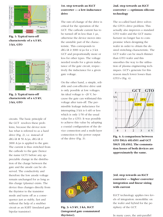
GTO has serious control issues and requires an unstable transition zone where both anode voltage and cathode current act simultaneously during shutdown, relying on buffer circuits for support. GCT breaks through this limitation through "hard drive" technology:
The rate of change of gate current reaches µ
(far exceeding GTO's 50 A/µ s), it can switch the current from the cathode to the gate before there is a significant change in the charge distribution between the gate and anode.
Directly switch the device from thyristor mode to transistor mode, with stable and fast turn off process, no need for buffer circuit, and performance close to IGBT.
(2) The Four Key Development Steps of IGCT Converter
Low inductance drive design
To avoid the GCT entering the unstable working zone, the cathode current needs to be turned off within 1 µ s, and the leakage inductance of the gate circuit corresponding to the 3kA GCT should be ≤ 6nH (only 1/50 of the conventional value of GTO).
Low inductance is achieved through a multi-layer connection between the coaxial device connection structure and the driving power output, while using a gate voltage of -20V to balance reliability and cost-effectiveness.
Optimize silicon wafer technology
Hard drive technology allows GCT silicon wafers to be designed thinner without compromising on switch characteristics, combined with plasma engineering technology, significantly reducing losses (compared to GTO of the same specification, the commutation loss is similar but the on state loss is lower).
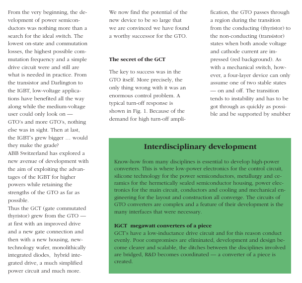
High integration and linear scaling of current
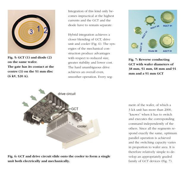
Integration is divided into two levels: one is single-chip integration (integrating anti parallel diodes and GCTs on the same silicon wafer to reduce diode stacking and high current connections); The second is hybrid integration (integrating GCT, driving unit, and cooler to reduce volume, improve stability, and lower costs).
Each unit of the silicon wafer (3kA devices containing over 2000 units) synchronously responds to switch instructions, achieving optimal parallel operation. The current capacity is linearly related to the silicon wafer area, making it easy to develop multi specification GCT series (such as devices with silicon wafer diameters of 38mm, 51mm, 68mm, and 91mm).
Simplify circuit complexity
No buffering capacitors, diodes, and resistors are required for GTO converters, only the current rise rate when GCT is turned on needs to be limited (as high-voltage silicon diodes are slower than low-voltage IGBT diodes).
By adopting a new high current circuit, all phases of the inverter can be connected to the same DC bus, which is comparable in cost to conventional IGBT converters.
(3) Modular design and high-voltage adaptation
Modular component system: In response to the diverse application requirements and small batch size of high-power converters, IGCT adopts modular design, which can cover a power range of 250kW to 100MW through unit series connection and adapt to different scenarios.
Pressure contact technology: Traditional module technology is difficult to handle high voltage and high current. IGCT adopts an improved pressure contact technology, which integrates the driving unit, power semiconductor, and cooler into a single functional unit. It replaces expensive chip parallel arrays with optimized silicon wafers in standard packaging, simplifies manufacturing, reduces costs, and is easy to maintain.
Performance advantages and application cases of IGCT converters
(1) Core performance advantages
Category specific advantages
Component characteristics include high rated voltage, low turn-on and commutation losses, high commutation frequency (intermittent up to 7kHz, average 500Hz for three-point converters, equivalent two-point 2kHz), high silicon wafer utilization, uniform current distribution, linear correlation between current capacity and silicon wafer area, and easy modeling
Circuit design includes a three-phase shared DC bus, a central dI/dt limiter with integrated clamping, simple intermediate circuit connection, safety and reliability under extreme working conditions, and a simple driving circuit (directly coupled with switch signals, no dV/dt or dI/dt regulation circuit required, dual line low-power power supply)
Overall performance with few and no special components, modular mechanical structure, single-chip integration even under high fixed values, high compatibility between power semiconductor control system cooler, stable and easy to center pressure contact technology, easy maintenance, efficiency exceeding 98%, high reliability (MTBF>6 years), small size and light weight, clear interface definition, support for high-power and reliable series operation, and series redundancy design to enhance reliability
(2) Typical application cases
100MW Bremen railway system interconnection device: put into operation in 1996, with 288 IGCTs running without faults, verifying the high reliability and series ease of use of IGCTs.
High dynamic application scenarios: such as uninterruptible power supply (NBPS), traction inverters, etc. Taking the ABB ACS1000 series medium voltage inverter as an example (launched in 1997 with a research and development cycle of only 2 years), it adopts a three-point IGCT inverter and a sine wave output filter, supports direct torque control (DTC), adapts to 2.3kV-4.16kV voltage and 315kW-5MW power range, and can be used for the transformation of existing non speed regulating motors. The debugging difficulty is comparable to that of low-voltage ACS600.
1.5MW air-cooled three-phase phase module: with a commutation frequency of 1050Hz, suitable for high-frequency demand scenarios.
Technological Development History and Future Prospects
(1) Development History (Key Nodes from 1993 to 2003)
1993: Hard drive GTO technology began;
In 1995, 3kA/4.5kV GCT was launched;
In 1997, 6kV/1kA reverse conducting diode (without buffer circuit) and transparent emitter technology were implemented, and the ACS1000 series inverter was launched;
Follow up: Gradually develop 4.5kV/6kA (91mm silicon wafer) GCT and 250A-4kA GCT series, achieve improvements such as integrated coolers and modular driver units, and expand application scenarios.
(2) Future prospects
IGCT technology has firmly established itself in the medium and high voltage field in just a few years, combining the advantages of GTO and IGBT to overcome their shortcomings. With excellent performance, reliability, and cost-effectiveness, IGCT will continue to expand high-power application scenarios and become one of the core technologies of medium and high voltage converters, further promoting the efficient and miniaturized development of the power electronics field.
- YOKOGAWA
- Reliance
- ADVANCED
- SEW
- ProSoft
- WATLOW
- Kongsberg
- FANUC
- VSD
- DCS
- PLC
- man-machine
- Covid-19
- Energy and Gender
- Energy Access
- Renewable Integration
- Energy Subsidies
- Energy and Water
- Net zero emission
- Energy Security
- Critical Minerals
- A-B
- petroleum
- Mine scale
- Sewage treatment
- cement
- architecture
- Industrial information
- New energy
- Automobile market
- electricity
- Construction site
- HIMA
- ABB
- Rockwell
- Schneider Modicon
- Siemens
- xYCOM
- Yaskawa
- Woodward
- BOSCH Rexroth
- MOOG
- General Electric
- American NI
- Rolls-Royce
- CTI
- Honeywell
- EMERSON
- MAN
- GE
- TRICONEX
- Control Wave
- ALSTOM
- AMAT
- STUDER
- KONGSBERG
- MOTOROLA
- DANAHER MOTION
- Bentley
- Galil
- EATON
- MOLEX
- Triconex
- DEIF
- B&W
- ZYGO
- Aerotech
- DANFOSS
- KOLLMORGEN
- Beijer
- Endress+Hauser
- schneider
- Foxboro
- KB
- REXROTH
- YAMAHA
- Johnson
- Westinghouse
- WAGO
- TOSHIBA
- TEKTRONIX
- BENDER
- BMCM
- SMC
- HITACHI
- HIRSCHMANN
- XP POWER
- Baldor
- Meggitt
- SHINKAWA
- Other Brands
- UniOP
- KUKA
- IBA
- Beckhoff
- ADLINK
-
ADLINK HPCI-14S12U - Industrial Control Backplane 12PCI Backplane PCI-14S Passive Backplane
-
ADLINK PCIe-GIE74C - image acquisition card 4-CH GigE Vision PoE+ Frame Grabber
-
ADLINK PCI-8164 - control card 4-Axis Advanced Motion Controller Board
-
ADLINK PCIe-U304 - 4 Port USB3 PCIe Frame Grabbers USB Screw Hole Card
-
ADLINK PCI-9112 - Multi-Function Data Acquisition Card DAQ Card
-
ADLINK PCI-7432 - 51-12013-0A50 4-CH Isolated Numérique I/O PCI Cartes Digital I/O Card
-
ADLINK PCA-6106P3-0C1 REV.C1 - backplane 6-Slot Passive Backplane Board
-
ADLINK PCI-7224 - 24-CH Opto-Isolated Digital I/O PCI Board
-
ADLINK CPCI-7433R(G) - Digital Input Board Rear I/O CompactPCI Card
-
ADLINK EBP-13E4 - 51-46703-0A30 Industrial PC Backplane Passive Backplane
-
ADLINK PCIE-HDV62 - Image acquisition card High Definition Video Frame Grabber
-
ADLINK EBP-13E4 - 51-46703-0A30 Industrial Backplane Board Passive Backplane
-
ADLINK 90111-B1 / CPCI-6770 - PCB CPU MODULE CompactPCI Single Board Computer
-
ADLINK PCI-7248 - DATA ACQUISITION PCI CARD 48-CH Parallel Digital I/O Board
-
ADLINK PCI-7230 - 51-12003-0a50 board PCI7230 32-CH Isolated Digital I/O Card
-
ADLINK PCI2A000CB - 51-20000-0B30 Multi-Function DAQ Card Baseboard
-
ADLINK PCI-8134-005 - 4-Axis Motion Controller Card
-
ADLINK PCI-7224 - 24-CH Opto-Isolated Digital I/O PCI Card
-
ADLINK PCI-7434 - 64-CH Isolated Digital Output Card
-
ADLINK PCI-8132 - motion control card 2-Axis Servo & Stepper Controller
-
ADLINK PCI-8134 - Motion Controller PCI Card 4-Axis Controller Board
-
ADLINK PCI-8164 - Motion Control Card 51-12406-0A40 4-Axis Controller
-
ADLINK 51-12001-0C20 - Circuit Board Data Acquisition Interface Module Hardware
-
ADLINK NuPR0-840 - industrial control motherboard Full-Size PICMG CPU Board
-
ADLINK PCI-7444 - 51-12023-0A10 card 128-CH Isolated Digital Output Board
-
ADLINK PCI-1612B - data acquisition card 4-Port RS-232/422/485 Serial Communication Card
-
ADLINK PCI-6208V 009 - 8/16-CH 16-Bit Analog Output Cards PCB-I-E-482=6BX3
-
ADLINK NUPRO-935A/LV - industrial control motherboard Full-Size PICMG SBC Board
-
ADLINK PCI-9114DG - Multi-Function DAQ Card Data Acquisition PCI Card
-
ADLINK ACL-7130 - Data acquisition card Isolated Digital I/O Board
-
ADLINK ABX-6300D-4E1-BP - board ABX6300D4E1BP Video Interface Expansion Card
-
ADLINK CPCI-6940 - CPCI-6940/D1539/M16-0(EA)-000E 6U CompactPCI Processor Board
-
ADLINK NuPRO-760 - industrial control motherboard Half-Size PICMG SBC CPU Board
-
ADLINK IMB-M42H (G)-0020 - industrial control motherboard LGA1155 Micro-ATX Mainboard
-
ADLINK RTV-24 / PCI-MP4S - 51-12519-1C30 4-Channel Real Time Video Capture Board
-
ADLINK PCI-8134 - 4-Axis Servo & Stepper Motion Controller Card
-
ADLINK MXC-6101D - V.PC000.002.ST.00 Box PC Configurable Embedded Computer
-
ADLINK PCI-8134A - 51-12421-0A10 Motion Control Card 4-Axis Controller Card
-
ADLINK DIN-100S / DIN-100SA1 - Technology SCSI-II TB 100-PIN Terminal Block Board
-
ADLINK DIN-812M001 / DIN812M001 - 51-14034-0A1 51140340A1 Terminal Module Breakout Interface
-
ADLINK PCI-8164 - Servo motion control 4-Axis Advanced Controller Card
-
ADLINK PCIe-GIE64 - Acquisition card GigE Vision PoE+ Frame Grabber
-
ADLINK M-302 - Industrial control motherboard ATX PC Board Mainboard
-
ADLINK PCI-8134 - Motion Controller PCI Card 4-Axis Controller Board
-
ADLINK PCI-RTV24 - Image capture card Analog Video Frame Grabber
-
ADLINK PCI-8102 - Motion control card 2-Axis Servo & Stepper Controller Board
-
ADLINK PCI-9112 REV.B1 - Card Multi-Function Data Acquisition Card
-
ADLINK HSI-DI32-M-N / HSL-TB32-M-DIN - Discrete I/O MODULE Distributed Automation Module System
-
ADLINK PCI-7296 - IO card REV.A3 96-CH Parallel Digital I/O Card
-
ADLINK DIN-814P-A4 / 814Y - terminal board Motion Control Interface Block
-
ADLINK DIN-814P-A4 - 51-14056-0A10 PCB-I-E-2736=ZA01 Screw Terminal Board Breakout
-
ADLINK M-322 - motherboard Industrial Control Computer Mainboard
-
ADLINK NUPRO-406 REV:B1 - industrial control motherboard Full-Size PICMG CPU Board
-
ADLINK AMP-204C - card DSP-Based 4-Axis Advanced Pulse-Train Controller
-
ADLINK HPCI14S REV.B1 - industrial computer baseboard 14-Slot Passive Backplane
-
ADLINK PCI-7250 - 8-CH Relay Output & 8-CH Isolated DI PCI Card
-
ADLINK EBP-13E2 - baseplate Passive Backplane Industrial Computer Chassis Board
-
ADLINK LPCI-3488A - PCI-GPIB card 51-12801-0A30 acquisition card IEEE-488 Interface Board
-
ADLINK PCI-6216V-GL - 51-12201-0C30 16-CH 16-Bit Voltage Analog Output Card
-
ADLINK ACL-8454 - 16-CH Isolated Digital I/O & 4-CH Counter Card
-
ADLINK HPCI-9S7U - backplane Passive Backplane Compatible with NuPRO-A301 852 841 842
-
ADLINK DAQ-2010-007 - Simultaneous-Sampling Multi-Function Data Acquisition Card
-
ADLINK MP-C154 - 51-64205-0A10 Motion Control Card 4-Axis Controller Board
-
ADLINK MXE-202/mSSD16B/WiFi-BT - Matrix Rugged I/O Platform Embedded Fanless Computer
-
ADLINK CM-920-R-17 - PC/104-Plus Single Board Computer Module Intel Celeron M
-
ADLINK PCI-7250 NSMP - 8-CH Relay Output & 8-CH Isolated DI Card
-
ADLINK PCI-8164 - 4-Axis Motion Controller PCI Card W/ Cable and Breakout Box
-
ADLINK EMX-100 - Ethernet-based 4-axis Motion Controllers Distributed Motion Module
-
ADLINK PCI-8134A - Press control card 4-Axis Motion Controller Board
-
ADLINK M-845EG REV:3.2 - industrial motherboard Pentium 4 Socket 478 Micro-ATX
-
ADLINK PCI-9114A Rev A2 DG - card High-Resolution Multi-Function Data Acquisition Board
-
ADLINK IEC-915GV - REV 1.1 Industrial motherboard Socket 478 CPU Board
-
ADLINK PCI-9111DG(G) - Data Acquisition Card Multi-Function DAQ Card
-
ADLINK HPCI-15S10 REV:B2 - Industrial computer base plate Passive Backplane Board
-
ADLINK NuPR0-840 / NuPR0-840DV - industrial control motherboard Full-size PICMG CPU Board
-
ADLINK RTV-24 / PCI-MP4S - 51-12519-1C30 4-Channel Real Time Video Capture Board
-
ADLINK NUPRO-780 - industrial control motherboard Pentium III Single Board Computer
-
ADLINK PCI-7296 - 0050 card 96-CH Opto-Isolated Parallel DIO Card Set
-
ADLINK NUPRO-780 - industrial control motherboard PICMG Full-Size SBC
-
ADLINK PCI-7248 - 51-12006-0A3 002 Pci 7248 48-CH Parallel Digital I/O Card
-
ADLINK PCI-7230 - 32-CH Isolated Digital I/O Card
-
ADLINK AMP-204C - motion control card 4-Axis Advanced Controller Board
-
ADLINK PCI-1714UL - Card Ultra High-Speed 4-CH Simultaneous Sampling DAQ
-
ADLINK NuPRO-E330 - industrial computer equipment motherboard PICMG 1.3 SHB SBC
-
ADLINK AMP-204C - DSP-Based 4-Axis Advanced Pulse-Train Motion Controller Module
-
ADLINK PCI-7256 - 001 51-12206-0A2 REV.A2 LPCI-7256 16-CH Latching Relay Output Card
-
ADLINK ND6050 - NUDAM DIGITAL I/0 MODULE Distributed I/O Unit
-
ASEM BM100 - Box PC Embedded Fanless Industrial Computer
-
ADLINK PCI-7250 - PCI Acquisition Card 8-CH Relay Output & Isolated DI Board
-
ADLINK PCI-8164 - Servo motion control 4-Axis Controller Card
-
ADLINK NuPRO-A40H - Industrial Motherboard 51-41807-1A30 OSP LGA1155 H61
-
ADLINK ADMAX X300 SERVER - 51066010-0A30 motherboard Multi-Processor Mainboard
-
ADLINK CMe-GIE62+ - 51-32903-0A30 control card PC/104-Plus GigE Vision Frame Grabber
-
ADLINK NUPRO-780 - industrial control motherboard Full-Size PICMG SBC CPU Board
-
ADLINK ETX-AT-N270-18/GKTEL - 51-71111-OB10 motherboard ETX CPU Module Board
-
ADLINK DIN-812M - interface module Terminal Block Connection Board
-
ADLINK IMB-M42H - industrial control motherboard LGA1155 Micro-ATX Mainboard
-
ADLINK PXIS-2508 - 8-slot 3U PXI Instrument Chassis Power Hardware Assembly
-
ADLINK AMP-208C - Motion Control card DSP-Based 8-Axis Pulse-Train Controller
-
ADLINK PCI-9111 / PCI-9111DG - Multi-Function Data Acquisition Card DAQ Board
-
ADLINK IEEE-488 GPIB card - Bus Interface Controller Communication Board
-
ADLINK RTV-24 - 51-12519-1C30 image acquisition card Video Frame Grabber Card
-
ADLINK TB-24P/24-01 - Board 24 Way Screw Terminal Breakout Board
-
ADLINK HSL-DI16DO16-DB-NN - 51-23015-0A40 Distributed Discrete I/O Module Set
-
ADLINK PCI-7442 - switch quantity card data acquisition card 64-CH Isolated Card
-
ADLINK ACL-7130 REV. B2 - industrial control capture card Isolated Digital I/O PCI Card
-
ADLINK PCI-6S / PCI6S - Backplane 6-Slot Passive Backplane Chassis Board
-
ADLINK ACL-8113A - card Isolated Digital Input Card
-
ADLINK CPCI-6208V-003 - board cPCI CompactPCI 8-CH Analog Output Card
-
ADLINK DIN-100S-01(G) - SCSI 100-Pin Terminal Block Interface Board
-
ADLINK PCI-7433 - Isolated Digital Input Card 64-CH
-
ADLINK PCI-9812 - Synchronous sampling analog input card High-Speed DAQ Board
-
ADLINK PCI-7434 REV.B1 - PLOTECH PCB-I-E-1182=6EX2 64-CH Isolated Digital Output Card
-
ADLINK PCIe-RTV24 - 51-18016-0A20 4-CH Real-Time Video Capture Card PCIe Frame Grabber
-
ADLINK PCI-8144 / PCI-8144N - Motion control card 4-Axis Stepper Motor Controller
-
ADLINK DIN-68S-01 - terminal board 68-Pin Connector Terminal Block
-
ADLINK MP-C154 - Motion control card 4-Axis Advanced Controller Card
-
ADLINK PCI-7248 (G) - Motherboard 48-CH Parallel Digital I/O Card
-
ADLINK MXE-1301(G) - Intel Atom D2550+NM10 MXE 1300 Series 93-4130-0030 Embedded Computer
-
ADLINK PRO-841 Rev 2.0 / PRO-060907000670 - CPU 2.26GHz & RAM Industrial PC Board
-
ADLINK cPCI-6626 - 6U CompactPCI 2.0 Blades i7-2710QE PCB-I-E-2570=9N41
-
ADLINK MXC-6322D(G) - Industrial Fanless Computer
-
ADLINK cPCI-8168-004 - CompactPci NulPC Motion Control Board 51-36402-0A3
-
ADLINK CPCI-7300[G] - COMPACTPCI Digital I/O Card Data Acquisition
-
ADLINK CPCI-6626/2710/M4G - COMPACTPCI COMPUTER BOARD
-
ADLINK cPCI-8168-009 - cPCI NulPC Motion Control Board
-
ADLINK cPCI-6626/2710/M4G - VME CPU Board Computer Board
-
ADLINK CPCI-R6200(G)-0040 - COMPACTPCI CONTROL BOARD

K-JIANG

Add: Jimei North Road, Jimei District, Xiamen, Fujian, China
Tell:+86-15305925923