
K-WANG
+086-15305925923
Service expert in industrial control field!


Product
Article
NameDescriptionContent
Adequate Inventory, Timely Service
pursuit of excellence


Ship control system
Equipment control system
Power monitoring system
Current position:
新闻动态
newS
Brand
GE IS220PSCAH1A IS220PSCAH1B Serial communication: 6 channels
GE IS220PSCAH1A IS220PSCAH1B Serial communication: 6 channels
GE IS220PSCAH1A IS220PSCAH1B Serial communication: 6 channels
The “SERR/RST Select” bit is used to select whether the WDT generates an SERR#
on the local PCI bus or a system reset. If this bit is set to “0”, the WDT will
generate a system reset. Otherwise, the WDT will make the local PCI bus SERR#
signal active.
The “WDT Enable” bit is used to enable the Watchdog Timer function. This bit
must be set to “1” in order for the Watchdog Timer to function. Note that since all
registers default to zero after reset, the Watchdog Timer is always disabled after a
reset. The Watchdog Timer must be re-enabled by the application software after
reset in order for the Watchdog Timer to continue to operate. Once the Watchdog
Timer is enabled, the application software must refresh the Watchdog Timer
within the selected timeout period to prevent a reset or SERR# from being
generated. The Watchdog Timer is refreshed by performing a write to the WDT
Keepalive register (WKPA). The data written is irrelevant.
3.4.2 WDT Keepalive Register (WKPA)
When enabled, the Watchdog Timer is prevented from resetting the system by
writing to the WDT Keepalive Register (WKPA) located at offset 0x0C from the
address in BAR2 within the selected timeout period. The data written to this
location is irrelevant.
3.5 NVRAM
The V7768/V7769 provide 32 KByte of non-volatile RAM. This memory is mapped
in 32K of address space starting at the address in BAR1. This memory is available
at any time and supports byte, short word and long word accesses from the PCI
bus. The contents of this memory are retained when the power to the board is
removed.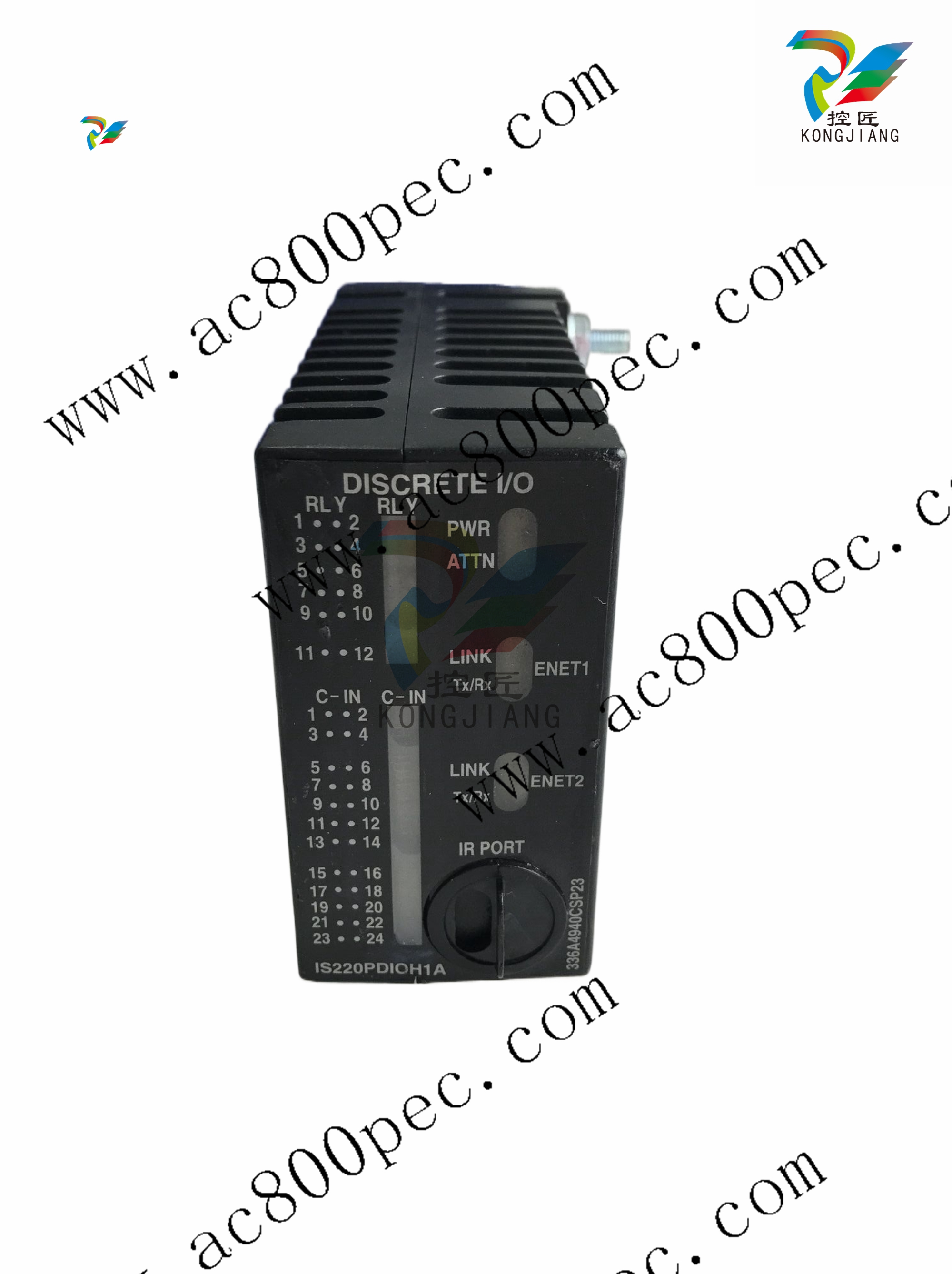
Table 3-13 Register Definitions Offset from BAR0
Register and Offset Bit Name Bit Definition
VMECOMM
Offset 0x00
MEC_SEL 0 Master Big-Endian Enable bit
1=Big Endian, 0=Little Endian
SEC_SEL 1 Slave Big-Endian Enable bit
1=Big Endian, 0=Little Endian
ABLE 2 Auxiliary BERR Logic Enable bit
1=Aux. BERR Enabled, 0=Aux. BERR Disabled
BTO 3 Bus Error Timer Enabled
1=Enable, 0=Disabled
BTOV [1:0] 5:4 Timeout Value
00 - 16 μs
01 - 64 μs
10 - 256 μs
11 - 1.00 ms
BERRI 6 BERR Interrupt Enable
1=Interrupt Enabled, 0=Interrupt Disabled
BERRST 7 BERR Status Read/Clear bit R/WC
1=Clear BERR status, 0=Do nothing
SFENA 8 Enables generation of VME SYSFAIL upon WDT
timeout
1=Enable SYSFAIL generation, 0=Disable
Unused 9 Not Used
BPENA 10 Endian Conversion Bypass bit
1=bypass, 0=Not bypassed
VBENA 11 VME Enable bit (VBENA)
1=Enabled, 0=Disabled
Unused 21:12 Not Used
VBAM
0x04
VME_ADD 5:0 Latched VME Address Modifier
Unused 31:6 Not Used
SEC_SEL 0x001
VBAR
0x08
VME_ADDR All Latched VME Address
- YOKOGAWA
- Reliance
- ADVANCED
- SEW
- ProSoft
- WATLOW
- Kongsberg
- FANUC
- VSD
- DCS
- PLC
- man-machine
- Covid-19
- Energy and Gender
- Energy Access
- Renewable Integration
- Energy Subsidies
- Energy and Water
- Net zero emission
- Energy Security
- Critical Minerals
- A-B
- petroleum
- Mine scale
- Sewage treatment
- cement
- architecture
- Industrial information
- New energy
- Automobile market
- electricity
- Construction site
- HIMA
- ABB
- Rockwell
- Schneider Modicon
- Siemens
- xYCOM
- Yaskawa
- Woodward
- BOSCH Rexroth
- MOOG
- General Electric
- American NI
- Rolls-Royce
- CTI
- Honeywell
- EMERSON
- MAN
- GE
- TRICONEX
- Control Wave
- ALSTOM
- AMAT
- STUDER
- KONGSBERG
- MOTOROLA
- DANAHER MOTION
- Bentley
- Galil
- EATON
- MOLEX
- Triconex
- DEIF
- B&W
- ZYGO
- Aerotech
- DANFOSS
- KOLLMORGEN
- Beijer
- Endress+Hauser
- schneider
- Foxboro
- KB
- REXROTH
- YAMAHA
- Johnson
- Westinghouse
- WAGO
- TOSHIBA
- TEKTRONIX
- BENDER
- BMCM
- SMC
- HITACHI
- HIRSCHMANN
- XP POWER
- Baldor
- Meggitt
- SHINKAWA
- Other Brands
- UniOP
- KUKA
- IBA
- Beckhoff
- ADLINK
91
-
Beckhoff AX5118-0000 - Servo Drive Module
-
Beckhoff CP2921-2000-0000 - Multi-Touch Control Panel
-
Beckhoff CX1020-0000 - CX1020-N000 CX1100-0001 Controller Set
-
Beckhoff CX8110 - 000007735 Embedded PC
-
Beckhoff CP7031-0002-0000 - CP-Link Interface Control 12.1" Panel
-
Beckhoff AX8118-0200-0000 - Single-Axis Module Motion Drive
-
Beckhoff CX2030-1020 - Basic CPU Module
-
Beckhoff CX5120-0125 - Embedded PC
-
Beckhoff CP2913-0000 - Multi-Touch Display 12.1" 1280 x 800 DVI USB 24VDC
-
Beckhoff CP6902-0001-0000 - Operator Interface 15" CP690200010000
-
Beckhoff ELM3502-0000 - EtherCAT Measurement Terminal 2-channel analog input
-
Beckhoff CX1030-0012 - CPU Module with CX1100-0014 CX1030-N041 CX1030-N030 N000
-
Beckhoff CP3915-0000 - 15" HMI Multi-Touch Panel
-
Beckhoff CU8803-0001 - CU8803-0000 Rev 2.2 Transmitter Box CP-Link 4
-
Beckhoff CX2030-0125 - CPU Module Embedded PC Windows PLC Controller
-
Beckhoff CX1020-0122-1001 - Multivac 105808023 CPU Module
-
Beckhoff CX2020-0121 - Embedded PC Module
-
Beckhoff KL3162 - PLC Module 2-channel analog input terminal
-
Beckhoff CP6607-0001-0020 - Built-in Panel PC Touchscreen 5.7" Arm Cortex-A8 1 GHz
-
Beckhoff EL3751 - EtherCAT Terminal 1 Channel Analog Input Multifunction 24 Bit
-
Beckhoff CX1010-0012 - CPU Module CX1010-0012
-
Beckhoff EL6631 - EtherCAT 2-Port Communication Interface Profinet RT Controller
-
Beckhoff C1510.1 - Interface Card
-
Beckhoff CX8080 - Embedded PC PLC Module
-
Beckhoff EL3218 - EtherCAT Terminal 8-Channel Analog Input
-
Beckhoff CP6700-0500 - Panel Control Flash PC Touch Screen 10.1" HMI
-
Beckhoff CP7011-1002-0010 - Polaris Operator HMI Display 30.5 cm
-
B&R 5AP920.1505-01 - TFT Display With Touch Screen
-
Beckhoff EL3351 - PLC Module Thermocouple Input Terminal
-
Beckhoff AM8052-0JH1-0000 - Servo Motor
-
Beckhoff CX5140-0135 - 4GB High-Performance Embedded Industrial PC
-
Beckhoff EP7211-0034 - EtherCAT Box 1 Channel Motion Interface
-
Beckhoff CX1020-0121 - CPU Module with CX1100-0002 CX1020-N010 N000
-
Beckhoff CX5140-0100 - 4GB Embedded PC
-
Beckhoff CP7711-0001-0030 - Industrial Computer Detection Panel
-
Beckhoff CX1020-0122 - CX1020-N030 CX1020-N010 CX1020-N000 CPU Module
-
Beckhoff CP6907-1000-0000 - Control Panel HMI
-
Beckhoff CX1020-0122 - CX1020-N030 CX1020-N000 CPU Module
-
Beckhoff CX2020-0123 - Embedded PC with CX2100 Power Supply
-
Beckhoff BX5100-0000 - Bus Terminal Controller Bus Coupler
-
Beckhoff C6930-0050 - Industrial Computer
-
Beckhoff CP6606-0001-0020 - Industrial Panel PC
-
Beckhoff CX9020-0115 - PLC Module CX90200115
-
B&R X20-SL-8000 - Ethernet Powerlink X20 Safety Controller Module Rev H0
-
Beckhoff CX2020-0155 - CPU Basic Module + Power Supply Module CX2100-0004
-
Beckhoff EJ7211-0010 - EtherCAT Plug-in Module Servomotor Motion Interface
-
Beckhoff C6920-0010 - Industrial PC Computer
-
Beckhoff CX1020-0112 - CPU Module with CX1020-N010 CX1020-N000 CX1100-0004
-
Beckhoff AX5203-0000 - Servo Driver Module
-
Beckhoff C6640-0050 - Industrial PC Intel Core i7-6700 3.4GHz CB1064-0002 Board
-
Beckhoff CX1020-0112 - CPU Module with CX1020-N000 CX1020-N010 CX1020-N030
-
Beckhoff CP6201-0001-0020 - Panel PC 24VDC
-
Beckhoff CX2020-0122 - Embedded PC Controller
-
B&R 5PC810.SX02-00 - Controller PC
-
B&R 4PP220.1043-K08 - REV G HMI Touch Panel 10.5in
-
B&R X20CP1586 - CPU Module
-
Beckhoff CX2040-0155 - Basic CPU Module Along with 40GB Card V 964
-
Beckhoff EL6652 - EtherCAT Terminal EtherNet/IP Master Scanner Rev 0018
-
Beckhoff C6650-0060 - Industrial PC
-
Beckhoff EP2328-0002 - EtherCAT Box 4-channel digital input 4-channel digital output
-
Beckhoff CX5120-0135 - Embedded PC CPU Module Intel Atom Processor 2GB RAM
-
Beckhoff CP7037-1037-0010 - Operator Interface Touchscreen
-
Beckhoff CX5140-0100 - 4GB Embedded PC
-
Beckhoff C5240-0020 - 000224115 Plc Module
-
Beckhoff CX5140-0100 - 4GB Embedded PC
-
Beckhoff EL2911 - 4 Channel Digital Input + 1 Channel Digital Output Module
-
Beckhoff CX1020-0000 - CX1020-N000 Automation Controller
-
Beckhoff CP2918-0000 - Control Panel HMI
-
Beckhoff CX2020-0122 - Embedded PC Controller
-
Beckhoff C6640-0040 - Control Cabinet Industrial PC 7-Slot
-
Beckhoff CP6201-0001-0020 - Touch Display Panel with Accessories
-
Beckhoff CP6207-0001-0020 - Panel PC 24VDC
-
Beckhoff C6930-1062-0050 - Control Cabinet Industrial PC
-
Beckhoff CP2712-1002-0000 - Baumann Automation Touch Control Panel
-
Beckhoff EL6631-0010 - EL66310010 Module PLC PROFINET RT Device
-
Beckhoff BK9000 - Ethernet TCP/IP Bus Coupler
-
Beckhoff CX5140-0175 - Embedded PC
-
Beckhoff CP2912-0000 - 12.1" Touch Screen Display CP29120000 24VDC
-
Beckhoff CP2712-1002-0000 - Baumann Automation Touch Control Panel
-
Beckhoff EK1100 - EtherCAT Coupler Reseller Lot of 38 with EK1122
-
Beckhoff KL1414 - 4-Channel Digital Input 24V DC 0.2ms 10 Piece Box
-
Beckhoff CP6533-0001-0060 - Control Cabinet PC Panel
-
Beckhoff EK9500 - EtherNet/IP Bus Coupler
-
Beckhoff CP6202-1047-0050 - Built-in Panel PC
-
Beckhoff C6017-0010 - Ultra-Compact Industrial PC Serial 000sndlk
-
Beckhoff C6650-0040 - Industrial PC
-
Beckhoff CX5230-0185 - 000119805 PLC Module 3D-71
-
Beckhoff EL3773 - Power Monitoring EtherCAT Terminal PLC Module
-
Beckhoff EL4732 - EtherCAT Terminal 2-channel analog output Pack of 10
-
Beckhoff CX1001-0120 - CPU Module cx10010120 cx1000-n001 cx1000-n000
-
Beckhoff CP6202-0001-0020 - Industrial Panel PC Atom Z530 32GB SSD 1GB RAM
-
Beckhoff CX5140-0175 - Embedded PC Intel Atom E3845 4GB RAM + 40GB CFast Card
-
Beckhoff EL3751 - EtherCAT Terminal 1 Channel Analog Input Multifunction 24 Bit
-
Beckhoff CP6202-0001-0010 - Economy Built-In Panel PC with HDD
-
Beckhoff C6320-M554 - Industrial PC
-
B&R 2AT300.6 - Analog Input Module 8x PT100
-
Beckhoff AX5206-0000-0202 - Digital Compact Servo Drive 2-axis
-
Beckhoff CX1020-0111 - CX1020-N000 CX1020-N010 CX1020-N030 CPU Module Bundle
-
Beckhoff CP6606-0001-0020 - Panel PC HMI
-
Beckhoff CX2020-0155 - CPU Basic Module + Power Supply Module CX2100-0004
-
Beckhoff CP2712-0000 - Panel 12.1" 24VDC CP27120000
-
Beckhoff C6150 - Control Cabinet PC
-
Beckhoff CP7711-0001-0030 - Industrial Computer Detection Panel
-
Beckhoff CP2913-0000 - Multi-Touch Display 12.1" 1280 x 800 DVI USB 24VDC
-
Beckhoff EK1322 - EtherCAT P Junction Module
-
Beckhoff CP6500-1012-0060 - 14250369 Control Cabinet PC
-
Beckhoff CP7902-0001-0000 - Control Panel HMI
-
Beckhoff EL6631-0010 - EL66310010 Module PLC PROFINET RT Device
-
Beckhoff CP2712-1002-0000 - Baumann Automation Touch Control Panel
-
Beckhoff C6920-0010 - Industrial PC Core Duo 2.00 GHz
-
Beckhoff C3640-0050 - Industrial PC
-
Beckhoff CX5140-0100 - 4GB Embedded PC
-
Beckhoff C6015-0010 - Ultra-Compact Industrial PC
-
Beckhoff KL3001 - PLC Module Analog Input Bus Terminal
-
Beckhoff CP7711-0001-0030 - Industrial Computer Detection Panel
-
Beckhoff AX5106-0000-0200 - Digital Compact Servo Drive 1-axis
-
Beckhoff CP2712-0000 - 12.1" 24VDC Touch Screen CP27120000
-
Beckhoff CP7037-1037-0010 - Operator Interface Touchscreen
-
Beckhoff CP7711-0001-0030 - Industrial Computer Detection Panel
-
Beckhoff C6220 - Industrial PC with Beckhoff FC3101 240 Volt
-
Beckhoff EL3164 - 4X Analog Input EtherCAT Terminal
-
Beckhoff C6140 - Husky PC 11 Industrial PC 160GB HDD Intel P3 850MHz w SERCOS 24V
-
Beckhoff KL6023-0000 - KL6023 EnOcean Wireless-Adapter
-
Beckhoff C3620-0000 - Industrial PC Motor Shelves
-
Beckhoff CX2020-0120 - PLC Module & CX2100-0004 PLC
-
Beckhoff Monitor - Industrial Display Screen
-
Beckhoff CP6020-0000-0000 - Touch Panel Screen
-
Beckhoff EK1960-0000 - TwinSAFE Compact Controller

K-JIANG

Add: Jimei North Road, Jimei District, Xiamen, Fujian, China
Tell:+86-15305925923