
K-WANG


Saia PCD4.U100 System Migration Complete Guide
However, a comprehensive replacement of the control system often means high costs and long downtime. Saia Burgess Controls (SBC) has launched the PCD4.U100 migration kit to address this pain point. This innovative solution allows users to upgrade the core processing unit to a more powerful PCD2.M5xxx or PCD3.Mxxxx series CPU while retaining the original PCD4 I/O module. This article will provide you with a detailed analysis of the hardware installation, address mode configuration, software migration process, and professional technical details of the PCD4.U100 suite based on official technical documents, and offer you a comprehensive operation guide.
Saia PCD4.U100 System Migration Complete Guide
Introduction: The inevitable choice for upgrading industrial control systems
In the field of industrial automation, lifecycle management of control systems has always been a core challenge faced by engineers. With the rapid iteration of technology, although the early Saia PCD4 series PLCs (programmable logic controllers) had excellent performance at the beginning of their design, their processing speed, memory capacity, and communication capabilities have gradually become limited in modern high demand application scenarios. In order to ensure the continuity of the production line and utilize the latest technological dividends, system upgrades have become inevitable.
However, a comprehensive replacement of the control system often means high costs and long downtime. Saia Burgess Controls (SBC) has launched the PCD4.U100 migration kit to address this pain point. This innovative solution allows users to upgrade the core processing unit to a more powerful PCD2.M5xxx or PCD3.Mxxxx series CPU while retaining the original PCD4 I/O module. This article will provide you with a detailed analysis of the hardware installation, address mode configuration, software migration process, and professional technical details of the PCD4.U100 suite based on official technical documents, and offer you a comprehensive operation guide.
Hardware migration architecture and compatibility review
A comprehensive review of the hardware compatibility of the existing system is the cornerstone of a successful migration before embarking on any physical operations. The core logic of the PCD4.U100 kit is to act as a "bridge" connecting the old PCD4 backplane bus with the new PCD2/PCD3 CPU bus.
1.1 Core Components and Connection Logic
The first step in migration work is the replacement of physical hardware. According to the official migration checklist, the standard operating procedure is as follows:
Remove old CPU: After power off, remove the old PCD4 CPU from the PCD4 rack. At this point, the PCD4. N2x0 power module must be retained on the rack as it serves as the foundation for system power supply.
Install PCD4.U100: Insert the PCD4.U100 module into the slot where the original CPU is located. This module serves as a bus converter.
Connect the new CPU: Use a dedicated connection cable to connect the PCD4.U100 to the new CPU.
If using a PCD2.M5xxx CPU, it is necessary to use a PCD2.K106 cable.
If using a PCD3.Mxxxx CPU, a PCD3.K116 or PCD3.K106 cable is required.
1.2 Key Compatibility Limitations
Not all old hardware can seamlessly support this upgrade, ignoring the following details may result in hardware damage or system failure:
Power module version: If a PCD4. N2x0 power module is used in the system, its hardware version must be Version B or a later version. The document clearly states that using older versions of power modules may cause irreversible physical damage to the PCD4.U100 module. This is because the new CPU has stricter requirements for power stability and startup timing.
CPU firmware requirements: The new PCD2.M5xxx or PCD3.Mxxxx CPU must be equipped with the NT-OS operating system, and the minimum firmware version requirement is 1.10.16. The old version of the operating system cannot recognize the bus mapping logic of PCD4.U100.
Unsupported modules: Not all I/O modules in the PCD4 series can be recognized by the new system. Especially the PCD4. HXxx series modules (usually specific high-voltage or special function modules) are not supported in this upgrade and must be removed or alternative solutions sought in the migration plan.
Serial interface: The original serial port of the PCD4 CPU will no longer be available, and the system will rely on the onboard serial interface of the new CPU (PCD2. M5 or PCD3) for communication.
Deep analysis of I/O address mode
The most complex and critical part of the PCD4.U100 kit is the configuration of the address mode. Due to the differences in the I/O addressing architecture between PCD4 and PCD3/PCD2, address conflicts must be coordinated through physical switches and software settings. There is a multi position switch on the back of the module for setting the starting address of the PCD4 I/O module.
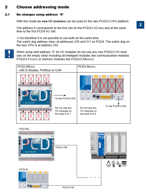
2.1 Mode 1: Starting Address' 0 '(No Change Mode)
This is the simplest configuration mode, suitable for scenarios where no new PCD2/3 I/O modules are intended to be added.
Switch position: Set the switch to Pos. 0 or Pos. 1.
Pos. 0: corresponds to situations where PCD2.M5xxx does not have an expansion module, or PCD3.Mxxxx has an expansion but no I/O module.
Pos. 1: Corresponding to the case of PCD3.M3xxx without expansion and no I/O module.
Address logic: The address of the PCD4 I/O module remains unchanged, starting from address 0.
Important limitation: In this mode, slot 0 of the new CPU (corresponding to slot 0-7 of PCD2.M5xxx and slot 0-4 of PCD3.Mxxxx) is logically occupied by PCD4 I/O. Therefore, it is strictly prohibited to insert new PCD2/3 I/O modules, including intelligent modules (such as communication module PCD2/3. Fxxx or memory module PCD2/3. R6xx), into these slots. If inserted, it will cause serious address conflicts.
Watchdog address: The watchdog of PCD4 is kept at addresses 255 and 511, while the watchdog of the new CPU is located at address 255. The system will maintain two watchdog instances.
2.2 Mode 2: Starting Address' 256 '(Extended Mode)
This mode provides the system with scalability, allowing users to utilize the new platform's scalability while retaining old I/O.
Switch position: Set the switch to Pos. 2 or Pos. 3.
Pos. 2: Suitable for PCD3.Mxxxx with expansion or PCD2.M5xxx without expansion, allowing up to 8 new PCD2/3 I/O modules to be used.
Pos. 3: Suitable for PCD3.Mxxxx without expansion, allowing up to 4 new PCD3 I/O modules to be used.
Address offset: All PCD4 I/O addresses will be offset backwards by 256 units as a whole. For example, the module originally with address 0 has now become 256.
Dual watchdog mechanism: In this architecture, the system will explicitly have two watchdog mechanisms. The watchdog of the new CPU is located at address 255, while the watchdog of the PCD4 system is mapped to addresses 511 and 767. Programmers must adapt to this change in the user program.
2.3 Address impact of serial communication
The address allocation for serial communication is also affected by the mode:
When using the onboard serial port of a new CPU and not using the PCD2/3 I/O module, the PCD4 I/O address range starts from 0.
When using PCD3. Fxxx or PCD2. Fxxx communication modules, these modules occupy the I/O address space, forcing the starting address of PCD4 I/O to automatically adjust to 256. This requires the user program to make corresponding code modifications.
Software environment upgrade and project migration
After the hardware connection is completed, the establishment of the software environment and project migration are the key to the system's "resurrection". Saia PG5 ® Control programming software is the core tool for this process.
3.1 Software version requirements
In order to support PCD4.U100 and the new CPU architecture, PG5 software must be updated to a specific version:
Saia PG5 ® 1.4.300: Patch 15 or higher must be installed.
Saia PG5 ® 2.0: SP1 (Service Pack 1) or higher must be installed.
3.2 Project Migration Steps
Backup: Before performing any operation, all old project files (PG3 or PG4 projects) must be fully backed up.
Project update: Open PG5 and import old projects. The software will automatically prompt to update the project structure.
Remove CPU specific features: Old projects may contain specific functional blocks or instructions for the PCD4 CPU that cannot be parsed in the new CPU and must be manually removed.
Hardware configuration: In the hardware configurator of PG5, change the CPU model to the actual new model used (PCD2.M5_ or PCD3. M0).
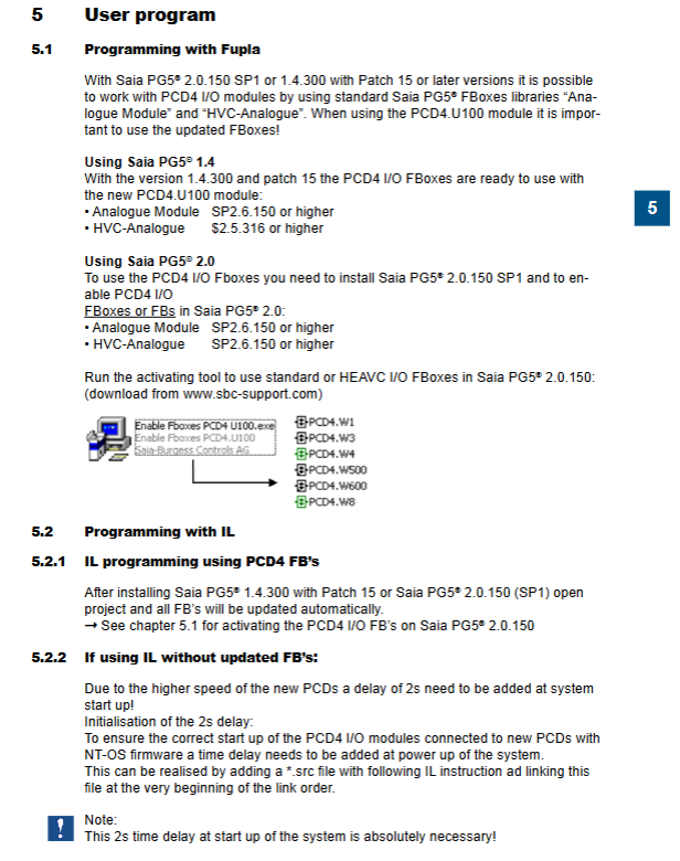
Activate FBox library: For PG5 2.0 users, the activation tool needs to be manually run to enable the FBox library for PCD4 I/O. This includes the "Analog Module" and the "HVC Analog" library. Only after activation can the software correctly recognize and control the I/O module of PCD4.
User program adaptation and IL code deep optimization
This is the most technologically advanced stage in the migration process. Due to the much higher running speed of the new CPU compared to the old PCD4, simple program porting often leads to timing errors or initialization failures. The manual provides a detailed list of adaptation schemes for instruction list (IL) programming.
4.1 The necessity of starting delay
Phenomenon: The startup speed of the new CPU is extremely fast, and it may start sending control instructions before the PCD4 I/O module completes its initialization, resulting in abnormal response of the I/O module.
Solution: A 2-second delay must be forcibly inserted at system startup.
Implementation method: Create a source file named Wait_2s.src and place it at the top of the link order. The code logic is as follows:
$INIT
ACC H
LD T 0
T#2s ; Set the delay time to 2 seconds
LOOP:
STH T 0
JR H LOOP
ACC H
$ENDINIT
Through this code, the program will loop and wait for timer T0 to reach 2 seconds during the initialization phase, ensuring that the modules on the PCD4 backplane have enough time to power on, reset, and be ready.
4.2 Timing correction of analog module (PCD4. W100)
PCD4.W100 is an analog module, and its A/D (analog-to-digital conversion) and D/A (digital to analog conversion) processes require specific physical time. On old CPUs, due to the longer instruction execution cycle, the program running speed naturally covers this delay. But on high-speed CPUs, continuous read and write instructions ignore the conversion time of modules.
Correction plan: Insert NOP (null operation) instruction between read and write operations.
Reading process: Select channel ->Start conversion ->Wait (STH I 15 detects high level) ->Read data. During this process, the insertion of NOP instructions prevents the CPU from polling status bits too quickly.
Writing process: Output data ->Select channel ->Start conversion ->Insert NOP. This ensures that the data is stably written into the module register before the next operation.
4.3 Initialization of Advanced Modules (PCD4. W500/W600)
For advanced modules such as PCD4.W500 and W600, simple delays are no longer sufficient to complete initialization and must be explicitly configured through specific functional blocks (CFB).
The control function block must be called in XOB 16 (initialization interrupt block):
Restart control: First, call CFB Control with parameter Restart warm (7) to perform a hot restart on the module.
Configuration download: Then call CFB config to write the configuration data block (DB) to the module.
If multiple W500 or W600 modules are used in the system, it is recommended to handle all restart instructions centrally, and then handle all configuration instructions centrally. This batch processing method can optimize initialization time and prevent system startup timeout.
System functional differences and exception handling
The upgraded system has subtle but significant differences in underlying logic compared to the old system, which engineers need to pay special attention to when debugging.
5.1 LED status indication
On the PCD4. N210 power/bus module, the functionality of some LED indicator lights has changed:
Effective LEDs:+24V,+5V (bus signal), Reset (restart signal), Watch Dog.
Failed LED: The battery indicator light, RUN/HALT operation indicator light, and CLEAR clear indicator light will no longer have their original functions after connecting to a new CPU. This is because these states are now directly managed by the indicator lights on the new CPU panel.
5.2 Exception Handling Block (XOB)
Abandonment of XOB 5: In the PCD4 system, XOB 5 is used to process/IOQUIT signals (I/O exit confirmation). The signal mechanism has been removed in the new CPU architecture, so the XOB 5 program block will no longer be executed. Suggest marking it as a comment when migrating code to avoid confusion.
The functional evolution of XOB 1: XOB 1 is used to detect I/O bus power failures. Combined with the PCD4. N210 power module, the detection capability of XOB 1 has been enhanced. It can not only detect+5V output, but also monitor+/-15V voltage and input voltage. The delay time for the system to detect the fault is about 500ms, which provides a basis for writing a fault safety program.
- YOKOGAWA
- Reliance
- ADVANCED
- SEW
- ProSoft
- WATLOW
- Kongsberg
- FANUC
- VSD
- DCS
- PLC
- man-machine
- Covid-19
- Energy and Gender
- Energy Access
- Renewable Integration
- Energy Subsidies
- Energy and Water
- Net zero emission
- Energy Security
- Critical Minerals
- A-B
- petroleum
- Mine scale
- Sewage treatment
- cement
- architecture
- Industrial information
- New energy
- Automobile market
- electricity
- Construction site
- HIMA
- ABB
- Rockwell
- Schneider Modicon
- Siemens
- xYCOM
- Yaskawa
- Woodward
- BOSCH Rexroth
- MOOG
- General Electric
- American NI
- Rolls-Royce
- CTI
- Honeywell
- EMERSON
- MAN
- GE
- TRICONEX
- Control Wave
- ALSTOM
- AMAT
- STUDER
- KONGSBERG
- MOTOROLA
- DANAHER MOTION
- Bentley
- Galil
- EATON
- MOLEX
- Triconex
- DEIF
- B&W
- ZYGO
- Aerotech
- DANFOSS
- KOLLMORGEN
- Beijer
- Endress+Hauser
- schneider
- Foxboro
- KB
- REXROTH
- YAMAHA
- Johnson
- Westinghouse
- WAGO
- TOSHIBA
- TEKTRONIX
- BENDER
- BMCM
- SMC
- HITACHI
- HIRSCHMANN
- XP POWER
- Baldor
- Meggitt
- SHINKAWA
- Other Brands
- UniOP
- KUKA
- IBA
- Beckhoff
-
Basler Electric DECS-250-CN1SN1N Automatic Voltage Regulator for Generator Excitation Control
-
ADLINK CPCI-6860A - 51-31310-OB10 industrial motherboard CompactPCI SBC
-
ADLINK AmITX-SL-G-H110 - 51-7A104-0A30 Mini-ITX Industrial Motherboard
-
ADLINK PXI-2005-003 - CPCI Industrial PC Data Acquisition Card Multi-Function DAQ
-
ADLINK DININ-814M - 51-14032-0A3D SCSI-100P cable connection Interface Terminal Board
-
ADLINK CPCI-3920NA/C2D15/M1G - 3U CompactPCI Intel Core 2 Duo Single Board Computer
-
ADLINK PCIE-8560 - 51-18014-0A20 Communication Card High Speed DAQ
-
ADLINK PCI-C154+ - Motion Control Card 4-axis Motion Controller Board
-
ADLINK PCI-RTV24 - image capture card Analog Video Frame Grabber
-
ADLINK NuPRO-842LV/P - 51-41360-0B30 Industrial Motherboard CPU Board
-
ADLINK cBP-3208/3208R - CPCI Board 3U 8-Slot CompactPCI Backplane
-
ADLINK PCI-8164 - 4-Axis Motion Controller PCI Card 51-12406-0A40
-
ADLINK PCIe-GIE64+ - 4-CH GigE Vision PoE+ Frame Grabber Video Capture Card
-
ADLINK CPCI-6860 / 6860A - CompactPCI Dual Xeon Single Board Computer
-
ADLINK IEC-915GV - REV 1.1 Industrial motherboard CPU Board
-
ADLINK ND-6520 - Technology RS-232 to RS-422RS-485 Converter NuDAM Module
-
ADLINK RTV-24 / PCI-MP4S - 51-12519-1C30 4-Channel Real Time Video Capture Board
-
ADLINK cPCI-6910 / cPCI-6910AM/M1G - cPCI-6910AM/DXL16/M1G/S80G(G)-3120 BOARD CompactPCI SBC
-
ADLINK NUPRO-A40H - Linghua 51-41807-1A30 Industrial Control Computer Motherboard
-
ADLINK USB-3488A - USB to GPIB INTERFACE USB-3488A(G) Controller Module
-
ADLINK PCI-8134A - motion control card 4-Axis Controller Card
-
ADLINK PCI-7432 - Board 32-Channel input / 32-output Isolated Digital I/O PCI Card
-
ADLINK PCI-8134A - 51-12421-0A10 motion controller card tested
-
ADLINK LPCIe-7230 - 32 CH Isolated Input/output Card 2 Interrupts Low Profile PCIe
-
ADLINK NuPRO-E340 - industrial computer motherboard 51-47807-0A30 PICMG 1.3 SHB
-
ADLINK PCI-7434 - High-speed Digital Acquisition Card 64-CH Isolated DO Card
-
ADLINK NuPRO-E330 - 51-41805-0A20 Indsutrial Board SHB Single Board Computer
-
ADLINK PCI-7248 - OPTO-22 48 CHANNEL DIO DIGITAL TTL/DTL I/O 51-12006-0A40 GP
-
ADLINK PCI-8134 - Motion control card 4-Axis Controller Card
-
ADLINK AMP-208C - Movimiento Control Tarjeta 51-12420-1A20 W/Expansión & Breakout
-
ADLINK PCI-8164 - 51-12406-0A40 PCB Board 4-Axis Motion Controller Card
-
ADLINK DIN-68Y-SGII / DIN-68M-J3A - Terminal Board Connector Interface Block
-
ADLINK PCIe-7432 - Technology 51-18402-0A10 PCIe Card With High Input Range
-
ADLINK PCI-8144 / PCI-8144N - Motion control card 4-Axis Stepper Controller Card
-
ADLINK HSL-HUB3/REPEATER - HIGH SPEED LINK EXTENSION MODULES Distributed Hub Module
-
ADLINK ND-6017 - Data Logging + Acquisition 8CH A/D input Mod NuDAM Module
-
ADLINK LPCIe-7250 - data acquisition card Low Profile 8-CH Relay Output Card
-
ADLINK PCI-7432 - I/O card 64-CH Isolated Digital Input Output PCI Card
-
ADLINK IMB-M43H - industrial control computer motherboard Q87 Chip Micro-ATX
-
ADLINK MP-C154 - Motion control Card 4-Axis Motion Controller Board
-
ADLINK PCI-RTV24 - image capture card Video Frame Grabber Card
-
ADLINK PCI-7250 - 8-CH Relay Output & 8-CH Isolated DI Card
-
ADLINK PCI-6308V - 8-CH 12-Bit Isolated Analog Output PCI Card PCB-I-E-1148=6EX2
-
ADLINK PCI-7248 - capture card 48-CH Opto-22 Compatible DIO Card
-
ADLINK HSL-AI16A02-M-VV - Analog Input Output Distributed Module
-
ADLINK NuPRO-A301 - Rev:1.4 NUPRO-A301 PICMG Full-Size Single Board Computer
-
ADLINK PCI-6208V-GL - 8-CH Voltage Analog Output PCI Card
-
ADLINK PCI-8134A - 51-12421-0A10 4-Axis Motion Controller Card
-
ADLINK MNET-S23 - TECHNOLOGY MNET S23 - SERVO DRIVER CONTROL MODULE
-
ADLINK M-342 - ATX I3 I5 I7 Q67 Industrial Motherboard
-
ADLINK NUPRO-780 - Industrial Motherboard CPU Board PICMG SBC
-
ADLINK MP-C154 / MP-C152 - 4-Axis Motion Control Card Pulse-Train Controller
-
ADLINK NuPRO-935A/LV10B0 - Motherboard 51-41802-0A10 GP w/RAM Industrial Control Board
-
ADLINK MP-C154 - Motion control card 4-Axis Motion Controller Mainboard
-
ADLINK PCI-7250 - PCI Acquisition Card 8-CH Relay Output Isolated DI Card
-
ADLINK ACL-7124 - Technology Inc.24 DIO Card Digital Input Output Card
-
ADLINK PCI-8554 A2 - Timer/Counter Data Acquisition Card
-
ADLINK DIN-825-GP4 - Terminal Block Interface Board Breakout Module
-
ADLINK NuPR0-761 - REV:1.1 Industrial motherboard Full-Size PICMG SBC
-
ADLINK MXE-1401/M8G (G) - Matrix Fanless Embedded Computer Industrial PC
-
ADLINK HSL-DI16DO16-UD-NN - Digital 16 Channel I/O Mod Distributed I/O Module
-
ADLINK ND6520 - NUDAM INTELLIGENT DA&C MODULE RS232-RS-422/RS485 CONVERTOR
-
ADLINK NUPRO-761 - REV:1.1 Industrial Motherboard CPU Board
-
ADLINK AMP-208C - Motion Control Card 51-12420-1A20 DSP-based 8-axis
-
ADLINK NuPRO-A301REV 1.4 - with packaging industrial computer motherboard PICMG SBC
-
ADLINK PCM-9112+ - 51-12300-0A2 industrial motherboard Multi-Function DAQ PC/104 Module
-
ADLINK PCM-7250+ - 8-CH Relay Outputs & 8-CH Isolated DI Module PC/104
-
ADLINK PCI-RTV24 - Image capture card Analog Video Frame Grabber
-
ADLINK PCI-8134 - Motion Controller PCI Card 4-Axis Controller Board
-
ADLINK PCI-7432 - Isolated Digital I/O PCI Card
-
ADLINK PCI-8554 A2 - acquisition card Timer/Counter Card
-
ADLINK PCI-8132 - Rev.A2 2-Axis Servo & Stepper Motion Controller Card
-
ADLINK PCI-8132 - Data Acquisition card 2-Axis Motion Controller Card
-
ADLINK EBP-13E4 - 51-46703-0A30 Industrial Backplane Board Passive Backplane
-
ADLINK PCI-800L - Electronic Card Interface Controller Card
-
ADLINK PCIe-GIE72 - 51-18531-0A10 PCB Board GigE Vision Frame Grabber
-
ADLINK DAQ-2010(G)-OOBO - Simultaneous-Sampling Multi-Function DAQ Card
-
ADLINK PCI-9112 - REV.B1 Multifunction DAQ Card Data Acquisition Card
-
ADLINK PCI-7230 - 51-12003-DA60 32-CH Isolated Digital I/O Card
-
ADLINK PCI-7432 - Data Acquisition Card Isolated Digital I/O PCI Card
-
ADLINK ETX-AT-N270-18/LXE - 51-71111-0A20 ETX CPU Module Motherboard
-
ADLINK HSL-DI32-UD-N - DIGITAL INPUT 32 POINTS MODULE Distributed I/O
-
ADLINK AMP-204C - Motion Control card DSP-Based 4-Axis Advanced Controller
-
ADLINK MNET-4XMOG-0050 - Four-axis Motion Controller Distributed Motion Module
-
ADLINK AMP-204C - Motion control card DSP-Based 4-Axis Pulse-Train Controller
-
ADLINK PCI-7442 - Switch card 64-Channel Datalogging & Acquisition Card
-
ADLINK M-302 - Industrial control motherboard ATX PC Board
-
ADLINK NUPRO-852 / NUPRO-852LV - Industrial motherboard Single Board Computer
-
ADLINK PCI-8134 - REV.B1. 4-Axis Motion Controller Card
-
ADLINK PCI-GIE62 + - 51-18502-0A20 2-CH GigE Vision Frame Grabber PoE Card
-
ADLINK PCI-MPG24 - 51-12523-0B20 MPEG4 Card Video Compression Hardware
-
ADLINK HSL-TB32-M-DIN - 32-CH I/O TERMINAL W/ HSL-AI16AO2-M-VV MODULE
-
ADLINK PCI-M114-GL - PCB Ver 2.1 Motion Controller Axis Card
-
ADLINK IMB-M40H - SYM76996H61 motherboard Industrial Computer Mainboard
-
ADLINK NUPRO-A40H - 51-41807-1A20 industrial control motherboard H61 Chip
-
ADLINK PCI-M114-GL - Axis Card Data Acquisition Card PCB VER2.2 Motion Controller
-
ADLINK PCI-8134 - Motion Controller PCI Card 4-Axis Controller Board
-
ADLINK PCI-8102 - Motion control card 2-Axis Servo & Stepper Controller
-
ADLINK NuPRO-841REV:3.0 - motherboard Industrial Control PC Board
-
ADLINK HSL-TB32-U-DIN REV A1 - Breakout Terminal Board Field I/O Module
-
ADLINK AMP-204C - Motion Control card DSP-Based 4-Axis Pulse-Train Controller
-
ADLINK NUPRO-A40H - 51-41807-1A20 industrial control motherboard H61 PC Board
-
ADLINK PCI-6308A / PCI-6308V - 51-12202-0A50 Isolated Analog Output Card
-
ADLINK AMP-204C - DSP-Based 4-Axis Advanced Pulse-Train Motion Controller
-
ADLINK PCI-7434 - Technology 64-Channel Isolated Digital I/O PCI Cards
-
ADLINK CPCI-6840 / CPCI-6840V / PM16/M1G-12G0 - CompactPCI Single Board Computer CPU Module
-
ADLINK PCIE-GIE74 - Motherboard Video Capture Card 51-18531-0A10 Frame Grabber
-
ADLINK NuPRO-E330 - industrial computer equipment motherboard Control Mainboard
-
ADLINK AMP-208C / 51-12420-1A20 - Motion Control Card W/ Expansion & Breakout Board
-
ADLINK HPCI-14S12U - industrial computer baseboard Passive Backplane 14 Slots
-
ADLINK PCI-8164 - 4-Axis Motion Controller PCI Card W/ 1x Cable, 1x Breakout Box
-
ADLINK PCIe-RTV24 - 51-18016-0A20 Image Acquisition Video Capture Card
-
ADLINK M-342 - 5 PCI ATX Motherboard Industrial PC Mainboard
-
ADLINK PCI-FIW64 - 4/2 Channel IEEE1394B Image Capture Card FireWire Frame Grabber
-
ADLINK PCI-7432 - digital IO card 64-CH Isolated Digital Input Output Card
-
ADLINK 51-12001-0C20 - Circuit Board PCI-7200 Data Acquisition Controller Card
-
ADLINK PXI-3920 - PXI 3U cPCI Industrial Controller Embedded System CPU Board
-
ADLINK NuPRO-841REV:2.0 - motherboard Industrial Control PC Board
-
ADLINK NuPro-E330 - 51-41805-0A20 PCB Industrial Control Computer Motherboard
-
ADLINK PCI-RTV24 - Image capture card Analog Video Frame Grabber
-
ADLINK PCI-7442 - Switch card 64-Channel Datalogging & Acquisition Card
-
ADLINK HPX-13S4 - device baseboard Passive Backplane Riser Card
-
ADLINK PCI-9112 REV A.1 - Multi Function DA&C Board Data Acquisition Card
-
ADLINK PCI-7248 - 51-12006-0A40 Card Control 48-CH Digital I/O Module
-
ADLINK CPCI-6860 / 6860A - motherboard CompactPCI Dual Xeon Single Board Computer
-
ADLINK DPAC-3020-11(G) - Embedded PC Automation Controller Machine Control Board
-
ADLINK NuPRO-841 REV:1.0 - industrial control motherboard CPU Board
-
ADLINK MNET-4XMOG-0050 - Four-axis Motion Controller MNET Motion Control Card

K-JIANG

Add: Jimei North Road, Jimei District, Xiamen, Fujian, China
Tell:+86-15305925923