
K-WANG
+086-15305925923
Service expert in industrial control field!


Product
Article
NameDescriptionContent
Adequate Inventory, Timely Service
pursuit of excellence


Ship control system
Equipment control system
Power monitoring system
Current position:
新闻动态
newS
Brand
GE VMIVME-2511 PROGRAMMABLE 110 BOARD
GE VMIVME-2511 PROGRAMMABLE 110 BOARD
GE VMIVME-2511 PROGRAMMABLE 110 BOARD
Each timer can be independently enabled by writing a “1” to the appropriate “Timer x
Enable” field. Similarly, the generation of interrupts by each timer can be
independently enabled by writing a “1” to the appropriate “Timer x IRQ Enable”
field.
If an interrupt is generated by a timer, the source of the interrupt may be determined
by reading the “Timer x Caused IRQ” fields. If the field is set to “1”, then the
respective timer caused the interrupt. Note that multiple timers can cause a single
interrupt. Therefore, the status of all timers must be read to ensure that all interrupt
sources are recognized.
A particular timer interrupt can be cleared by writing a “0” to the appropriate “Timer
x Caused IRQ” field. Alternately, a write to the appropriate Timer x IRQ Clear (TxIC)
register will also clear the interrupt. When clearing the interrupt using the “Timer x
Caused IRQ” fields, note that it is very important to ensure that a proper bit mask is
used so that other register settings are not affected. The preferred method for clearing
interrupts is to use the “Timer x IRQ Clear” registers described on page 52.
Timer Control Status Register 2 (TCSR2)
The timers are also controlled by bits in the Timer Control Status Register 2 (TCSR2)
located at offset 0x04 from the address in BAR2. The mapping of the bits in this
register are as follows:
The “Read Latch Select” bit is used to select the latching mode of the programmable
timers. If this bit is set to “0”, then each timer output is latched upon a read of any one
of its address. For example, a read to the TMRCCR12 register latches the count of
timers 1 and 2. A read to the TMRCCR3 register latches the count of timer 3. This
continues for every read to any one of these registers. As a result, it is not possible to
Clock Rate MSb LSb
2MHz 0 0
1MHz 0 1
500kHz 1 0
250kHz 1 1
Field Bits Read or Write
Read Latch Select TCSR2[0] R/W
Reserved All Other Bits R/W
All of these bits default to “0” after system reset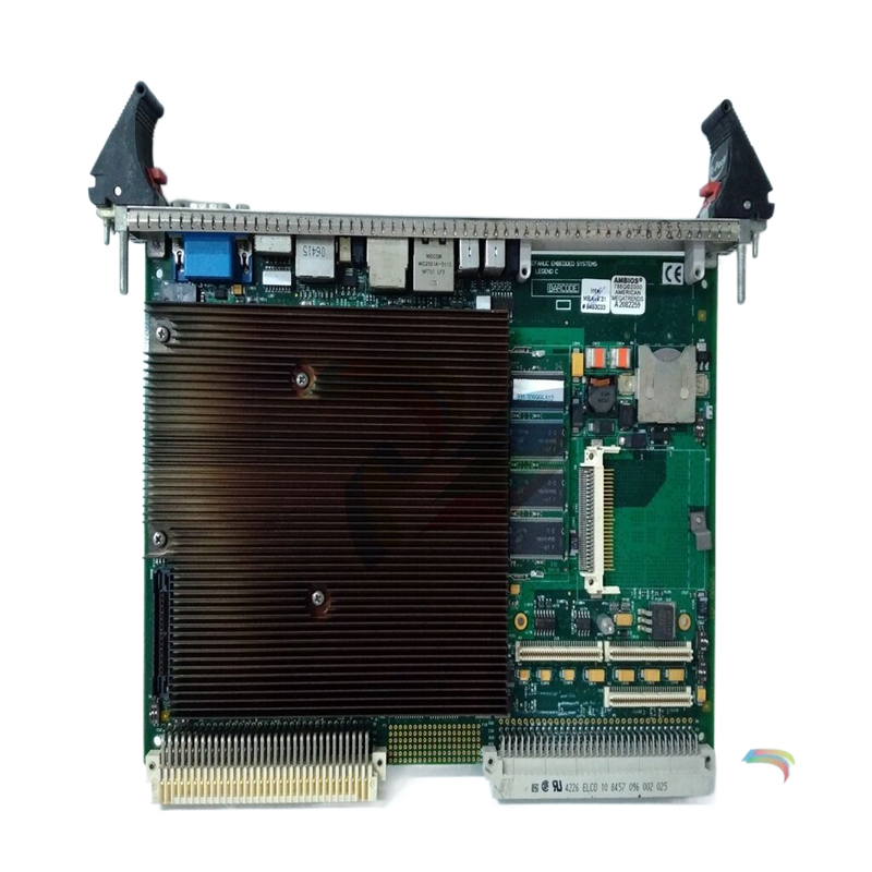
capture the values of all four timers at a given instance in time. However, by setting
this bit to “1”, all four timer outputs will be latched only on reads to the Timer 1 & 2
Current Count Register (TMRCCR12). Therefore, to capture the current count of all
four timers at the same time, perform a read to the TMRCCR12 first (with a 32-bit
read), followed by a read to TMRCCR3 and TMRCCR4. The first read (to the
TMRCCR12 register) causes all four timer values to be latched at the same time. The
subsequent reads to the TMRCCR3 and TMRCCR4 registers do not latch new count
values, allowing the count of all timers at the same instance in time to be obtained.
Timer 1 & 2 Load Count Register (TMRLCR12)
Timers 1 & 2 are 16-bits wide and obtain their load count from the Timer 1 & 2 Load
Count Register (TMRLCR12), located at offset 0x10 from the address in BAR2. The
mapping of bits in this register are as follows:
When either of these fields are written (either by a single 32-bit write or separate
16-bit writes), the respective timer is loaded with the written value on the next rising
edge of the timer clock, regardless of whether the timer is enabled or disabled. The
value stored in this register is also automatically reloaded on terminal count (or
timeout) of the timer.
Timer 3 Load Count Register (TMRLCR3)
Timer 3 is 32-bits wide and obtains its load count from the Timer 3 Load Count
Register (TMRLCR3), located at offset 0x14 from the address in BAR2. The mapping
of bits in this register are as follows:
When this field is written, Timer 3 is loaded with the written value on the next rising
edge of the timer clock, regardless of whether the timer is enabled or disabled. The
value stored in this register is also automatically reloaded on terminal count (or
timeout) of the timer.
Field Bits Read or Write
Timer 2 Load Count TMRLCR12[31..16] R/W
Timer 1 Load Count TMRLCR12[15..0] R/W
Field Bits Read or Write
Timer 3 Load Count TMRLCR3[31..0] R/W
- YOKOGAWA
- Reliance
- ADVANCED
- SEW
- ProSoft
- WATLOW
- Kongsberg
- FANUC
- VSD
- DCS
- PLC
- man-machine
- Covid-19
- Energy and Gender
- Energy Access
- Renewable Integration
- Energy Subsidies
- Energy and Water
- Net zero emission
- Energy Security
- Critical Minerals
- A-B
- petroleum
- Mine scale
- Sewage treatment
- cement
- architecture
- Industrial information
- New energy
- Automobile market
- electricity
- Construction site
- HIMA
- ABB
- Rockwell
- Schneider Modicon
- Siemens
- xYCOM
- Yaskawa
- Woodward
- BOSCH Rexroth
- MOOG
- General Electric
- American NI
- Rolls-Royce
- CTI
- Honeywell
- EMERSON
- MAN
- GE
- TRICONEX
- Control Wave
- ALSTOM
- AMAT
- STUDER
- KONGSBERG
- MOTOROLA
- DANAHER MOTION
- Bentley
- Galil
- EATON
- MOLEX
- Triconex
- DEIF
- B&W
- ZYGO
- Aerotech
- DANFOSS
- KOLLMORGEN
- Beijer
- Endress+Hauser
- schneider
- Foxboro
- KB
- REXROTH
- YAMAHA
- Johnson
- Westinghouse
- WAGO
- TOSHIBA
- TEKTRONIX
- BENDER
- BMCM
- SMC
- HITACHI
- HIRSCHMANN
- XP POWER
- Baldor
- Meggitt
- SHINKAWA
- Other Brands
- UniOP
- KUKA
- IBA
- Beckhoff
- ADLINK
91
-
Beckhoff EP9224-0037 - 4-Channel Power Distribution Box EtherCAT
-
Beckhoff CX2900-0026 - Solid State Flash Memory Card 20GB CFast
-
Beckhoff BK7500 - SERCOS Interface Fieldbus Bus Coupler Terminal
-
Beckhoff Ep2328-0002 - 4-Channel Input 4-Channel Output EtherCAT Box IP67
-
Beckhoff CX1020-0111 - Controller Kit Combo Interface Modules
-
B&R X20AI2237 - X20 System Analog Input Interface Module
-
Beckhoff CP2221-0010 - Multi-Touch Built-In Panel PC Touchscreen
-
Beckhoff CX1500-M310 - Fieldbus Master Interface Module 24V
-
Beckhoff CX2100-0904 - Power Charging Module Smart UPS Extension
-
Beckhoff CP3918-0000 - Multi-Touch Control Panel 18.5-Inch Monitor
-
Beckhoff CP2915-0000 - 15-Inch Multi-Touch Built-In Control Panel
-
Beckhoff CP7037-1027 - HMI Industrial Control Panel Built-In PC
-
Beckhoff EL3152 - 2-Channel Analog Input Terminal 4-20mA EtherCAT
-
Beckhoff CP6607-0000-0020 - 5.7-Inch Built-In Panel PC HMI Touch
-
Beckhoff EJ1809-0000 - 16-Channel Digital Input Pluggable Signal Level Terminal
-
Beckhoff AM8563-0N10-0000 - Synchronous Servo Motor
-
Beckhoff AX2006-S60600-520 - Compact Servo Drive Inverter
-
Beckhoff AM8053-0K20-0000 - Servo Motor with Planetary Gearbox AG3210
-
Beckhoff AM8042-0FH1-0000 - Synchronous Servo Motor
-
Rexroth R911338600 - IndraControl V HMI Terminal Beckhoff PCI Card FC9002
-
Beckhoff AX5125-0000 - 3 Phase Industrial Servo Drive 1000Hz
-
Beckhoff EP2328-0002 - 4-Channel Digital Input 4-Channel Output EtherCAT Box
-
B&R 7CP476-02 - System 2005 RTD CPU Module 3IF681.86 Interface
-
Beckhoff AX8620-0000-0000 - Power Supply Module Axis Drive System
-
Beckhoff CX1010-0111 - PLC Module CPU Controller 24V
-
Beckhoff AM8043-0H10-0000 - Synchronous Servo Motor
-
Beckhoff C6240-1009 - Control Cabinet Industrial PC Mainframe
-
Beckhoff BX8000-0000 - Bus Terminal Controller HW 4.4 Standalone
-
Beckhoff CP7721-1089-0020 - 12.1-Inch Touch Screen HMI Panel PC
-
Beckhoff CP7132-0001 - Industrial Built-In Panel PC Screen
-
Beckhoff CP2912-0010 - Multi-Touch Built-In Control Panel Display
-
Beckhoff CP2915-0000 - 15-Inch Multi-Touch Built-In Control Panel
-
Beckhoff AM8532-1EN0-0000 - Synchronous Servo Motor
-
Beckhoff AX5203-0000 - 2-Channel Digital Compact Servo Drive
-
Beckhoff CX2020-0141 - Embedded PC Core CPU Module
-
Beckhoff CP6832-0002-0010 - Built-In Industrial Control Panel Display
-
Beckhoff CX5020-0112 - Embedded PC CPU Control Module
-
Beckhoff CX5140-0175 - 4GB Embedded PC CPU Unit 24V
-
Beckhoff EL3681-0030 - Digital Multimeter Calibration Terminal EtherCAT
-
Beckhoff CP7201-1000-0000 - Industrial PC Touch Screen HMI Monitor
-
Beckhoff CP7232-1001-0000 - Industrial Panel PC Touch Screen
-
Beckhoff C6930-1032-0040 - Control Cabinet Industrial PC System
-
Beckhoff AX5125-0000 - 3 Phase Industrial Servo Drive 1000Hz
-
Beckhoff CP3916-1424-0000 - Multi-Touch Built-In Control Panel
-
B&R 1900071142 - Lemoine Fieldbus Communication Interface Module
-
Beckhoff EL2872 - 16-Channel Ribbon Cable Digital Output Terminal
-
Beckhoff CX2030-0120 - Embedded PC CPU Base Module Controller
-
Beckhoff CP3919-0000 - 19-Inch Multi-Touch Control Panel Touchscreen
-
Beckhoff AX5101-0000-0202 - Servo Driver Compact Intelligent Drive 180V
-
Beckhoff CX5130-0135 - Embedded PC Controller Module
-
Beckhoff CP3719-1061-0010 - Multi-Touch Panel PC Outer Housing Enclosure
-
Beckhoff CP3919-1033-0000 - 19-Inch Touch Industrial Panel Keyboard
-
Beckhoff CX5020-0111 - Embedded PC PLC CPU Module
-
Beckhoff FC5102-0000 - 2-Channel CANopen PCI Control Board Card
-
Beckhoff CX9001-1101 - Embedded PC CPU Network I/O System Module
-
Beckhoff CX1100-0920 - Smart Position Sensor Interface Module
-
B&R 4P3040.01-490 - Operator Panel PLC Interface Communication Module
-
Beckhoff CP2612-0000 - Dual-Touch Built-In Panel PC HMI
-
Beckhoff CP7002-1043-0010 - Touchscreen Display HMI Panel Terminal
-
Beckhoff CX9020-0115 - Embedded PC Controller Module
-
Beckhoff CX5140-0155 - 4GB Embedded PC CPU Module Die Industry
-
B&R 7DI435.7 - System 2005 Universal Digital Input Output Module
-
Bihl+Wiedemann BWU1568 - AS-i Master to Profibus Gateway Module
-
Beckhoff C6920-0070 - Control Cabinet Industrial PC 8GB Win 10
-
B&R X20AI2322 - 2-Channel Temperature Analog Input Module
-
Beckhoff CP2912-0000 - 12-Inch Touchscreen Display Monitor Screen
-
Beckhoff CP6022-1001-0010 - 15-Inch Built-In Control Panel
-
Beckhoff AM8031-0D10-0000 - Synchronous Servo Motor
-
Beckhoff CX5010-0111 - Embedded PC Controller CPU Module
-
Beckhoff CP7232-1000-0000 - Industrial Panel PC Touch Display Screen
-
Beckhoff CP7802-0011-0000 - 15-Inch Industrial Touchscreen Control Panel
-
Beckhoff C6320 - Control Cabinet Industrial PC
-
Beckhoff CX1030-0012 - Basic CPU Module Windows CE 6.0
-
Beckhoff CP2919-0000 - Installation Multi-Touch Control Panel
-
Beckhoff CX1020-0000 - Controller Set Stack System Pack
-
B&R 3DO480.6 - System 2005 Digital Output Module
-
Beckhoff EL3101 - 1-Channel Analog Input Terminal Differential +/-10V
-
Beckhoff AX8108-0200-0000 - Axis Feed Module Servo Drive
-
Beckhoff CP7802-1241-0010 - 15-Inch Industrial Touchscreen Control Panel
-
Beckhoff FC2002-0000 - 2-Channel Lightbus Data Acquisition PCI Card
-
Beckhoff CX5120-0155 - 2GB Embedded PC Intel Atom Controller
-
Beckhoff Cx9020-0111 - 1GB Basic CPU Module Embedded PC
-
Beckhoff CP6901-0001-0000 - 12-Inch Economy Built-In Control Panel
-
Beckhoff CX9020-0111 - Embedded PC CPU Basic Module
-
Beckhoff CX5130-0100 - 4GB Embedded PC CPU Module
-
Beckhoff CP2715-0010 - Multi-Touch Built-In Panel PC
-
Beckhoff CX2033-0175 - Embedded PC CPU Module Core i7
-
Beckhoff CP7201-1000-0000 - 12-Inch Touchscreen Panel PC AMAT Green Box
-
Beckhoff EL4038 - 8-Channel Analog Output Terminal 0-10V EtherCAT
-
Beckhoff CP6802-0000-0000 - Built-In Control Panel HMI Screen
-
Beckhoff AM8042-0F21-0000 - Synchronous Servo Motor
-
Beckhoff CX5120-0141 - Embedded PC Basic Controller Module
-
Beckhoff C6930-0050 - Control Cabinet Industrial PC System
-
Beckhoff CP6831-0002-0000 - Built-In Industrial Control Panel
-
Beckhoff CP6919-0001-0000 - Built-In Control Panel Display Unit
-
Beckhoff CP7201-1019-0030 - Built-In Panel PC HMI Monitor Screen
-
Beckhoff CP6809-0001-0000 - 6.5-Inch Touch Panel ELO Accutouch HMI
-
Beckhoff CX1020-0000 - Control Kit Combo Stack Units
-
Beckhoff cp3918-1012-0000 - 18.5-Inch Multi-Touch Control Panel
-
Beckhoff CX5140-0123 - 4GB Embedded PC CPU Module
-
Beckhoff C3230TP - Industrial PC Rackmount Workstation
-
Beckhoff CP6801-1006-0010 - Touch Panel HMI Display Unit
-
Beckhoff CX8010 - Embedded PC Controller Module
-
Beckhoff CP7011-0001 - Control Panel CRT Operator Pendant Monitor HMI
-
Beckhoff CX1010-0111 - Embedded PC CPU PLC Module 24V
-
Beckhoff CP2915-0000 - 15-Inch Multi-Touch Built-In Control Panel
-
Beckhoff CP7802 - Industrial Touch Screen Control Panel Monitor
-
Siemens 6AV7452-1AB00-0FB0 - Industrial PC Panel 877 Beckhoff PCI Cards
-
Beckhoff CP2612-0000 - Dual-Touch Integrated Panel Monitor Screen
-
Beckhoff CX5140-0175 - Embedded PC Core Controller
-
Beckhoff Cp6202-0001-0010 - Economy Built-In Panel PC System
-
Beckhoff C6320-0010 - Control Cabinet Industrial PC Unit
-
Beckhoff CP2919-0000 - Multi-Touch Built-In Control Panel Screen
-
Beckhoff CX9020-0111 - Embedded PC CPU Controller Module
-
B&R 3BP151.41 - System 2005 Backplane Base Module
-
Siemens 6AV7452-1AB00-0FB0 - Panel PC 877 with Beckhoff Communication Cards FC3101 FC7501
-
Beckhoff CX9001-1101 - Embedded PC System Fieldbus Module Bundle
-
Beckhoff CX1001-0122 - CPU Module PLC Controller 128MB RAM
-
Beckhoff CX5130-0175 - Embedded PC CPU Module Intel Atom Storage Card
-
Beckhoff C6140 - Industrial PC Tower Casing Pent 4 System
-
Beckhoff CX5020-0120 - Embedded PC Controller Core Module
-
Beckhoff C6017-0010 - Ultra-Compact Industrial PC
-
Beckhoff CP6809-0000-0000 - 6.5-Inch Industrial Panel Control Display
-
Beckhoff AX5021-0000-0000 - Brake Chopper Module Axis System
-
Beckhoff AM8031-0D10-0000 - Synchronous Servo Motor
-
Beckhoff CX8010 - Embedded PC Microcontroller Module
-
Beckhoff CP6202-1070-0070 - Built-In Panel PC HMI Touchscreen
-
Beckhoff C6920-0000 - Control Cabinet Industrial PC Module

K-JIANG

Add: Jimei North Road, Jimei District, Xiamen, Fujian, China
Tell:+86-15305925923