
K-WANG


TEKTRONIX VX4240 VXIbus protocol waveform digitizer/analyzer module
TEKTRONIX VX4240 VXIbus protocol waveform digitizer/analyzer module
Product identity and applicable scenarios
Tektronix VX4240 is a modular waveform digitizer/analyzer based on the VXIbus protocol, designed specifically for C or D-sized VXIbus mainframes. Its core positioning is a high-precision, multifunctional signal measurement and analysis tool. It integrates a 12 bit A/D converter and RISC processor, which can be widely used in laboratory signal testing, industrial equipment monitoring, electronic system development, and other scenarios. It can complete the entire process of capturing, storing, and analyzing DC to high-frequency AC signals.
Detailed explanation of core technical parameters
1. Hardware core configuration
Specific specifications of hardware components
A/D converter with 12 bit resolution, 10 MHz sampling rate, supports high-precision conversion from analog signals to digital signals
The INMOS T800 floating-point transputer processor is responsible for signal analysis and module control
Memory configuration standard 256K word sampling memory; Optional 512K word (Option 01) or 1M word (Option 02) expansion memory
Storage module with 128K bytes of RAM (running memory) and 128K bytes of EPROM (program storage); Non volatile memory (storing calibration parameters)
Two BNC input interfaces (SIG IN+, SIG IN -) and one DB25S connector (S3) for input/output; Support TTL level triggered input/output, clock input/output, ARM input/output
2. Key parameters for signal capture
(1) Frequency and Sampling Performance
Frequency range: DC to 5 MHz, with a attenuation index of -3 dB ± 1 dB at the 5 MHz frequency point, a roll off of -6 dB/octave in the 5-10 MHz frequency band, and a roll off of -18 dB/octave in the 10-20 MHz frequency band.
Sampling frequency: Programmable range from 0.005 Hz to 10 MHz, supports three clock sources - internal clock, external clock (TTL level, 50 Ω load, DC to 10 MHz), VXIbus 10 MHz ECL clock.
Sampling interval: 100 ns to 200 s (100 ns step) in internal/external clock mode, with a minimum period of 100 ns for external clock.
Clock accuracy: The internal clock has an annual drift of 5 ppm, ensuring long-term sampling stability.
(2) Input feature configuration
Voltage range:
Calibration range: ± 0.5 V, ± 1 V, ± 2 V, ± 5 V, ± 10 V, ± 20 V, ± 50 V, ± 100 V (8 levels in total, higher accuracy).
Virtual range: Supports any non calibrated voltage range within 100V, and achieves 12 bit weight allocation through Tek's self-developed virtual range circuit, with better performance than some 14 bit digitizers.
Input type: differential input (CMRR common mode rejection ratio:>40 dB from DC to 1 kHz, typical value for 50 Ω load>50 dB, typical value for 1 M Ω load>60 dB), single ended input.
Coupling methods: AC coupling, DC coupling, and grounding are available, suitable for different signal types (such as AC coupling isolating DC components).
Input impedance:
50 Ω (± 1%, parasitic capacitance<20 pF): suitable for high-frequency signal measurement.
1 M Ω (± 3%, parasitic capacitance<20 pF): suitable for measuring low-frequency and high impedance signals.
929 k Ω (± 2%, parasitic capacitance<20 pF): Suitable only for voltage ranges of 50 V and 100 V.
Resolution (12 bits): The smaller the voltage range, the higher the resolution, such as 0.48828 mV/bit for ± 1 V range and 48.828 mV/bit for ± 100 V range.
(3) Trigger and delay control
Trigger source: Supports 5 types of trigger sources, which can be flexibly combined (AND/OR logic of any two trigger sources):
External TTL edge trigger (programmable positive/negative edge).
Dual voltage threshold triggering (± 0 to ± 100% full-scale, 8-bit resolution).
VXIbus TTL trigger (8-channel programmable trigger line selection).
The VXIbus command is triggered.
Software triggering (receiving T command to start).
Trigger mode:
Pre trigger (CP): Store data before triggering and store a specified number of samples after triggering.
Post trigger (CT): default mode, data is stored after triggering, and the default sample size is memory size -100.
Central Trigger (CC): The trigger event is located in the center of the memory, with half of the samples stored before and after.
Free Run (CF): Uncontrolled by trigger control, continuously sampling after receiving the T command until receiving the stop command.
Record mode (CR): Automatic re triggering, storing data according to the set number of samples/records, supporting up to 65534 records.
Trigger delay: Programmable range of 200 ns to 420 s (200 ns step), delay uncertainty ≤ 200 ns+1 sampling clock cycle, meeting the requirements of precise timing control.
Trigger heavy arming time: In recording mode, it is one sampling clock cycle and supports fast continuous sampling.
3. Signal analysis function (40+core functions)
(1) Time domain analysis function
Function Name Description
Calculate the difference between the steady-state high level (100% point) and steady-state low level (0% point) of the signal using peak to peak voltage (AK), and return the maximum/minimum/average values
Rise time (AR) measures the time it takes for a signal to rise from 10% steady state to 90% steady state, and returns the maximum/minimum/average values
Falling time (AF) measures the time it takes for a signal to drop from 90% steady state to 10% steady state, and returns the maximum/minimum/average values
Return the maximum/minimum/average value and corresponding address of the part where the overshoot (AO) signal exceeds 100% steady-state value
Return the maximum/minimum/average value and corresponding address for the part of the down rush (AU) signal below 0% steady-state value
Find the maximum/minimum voltage values and corresponding memory addresses within the specified sample range (AX/AM)
Pulse width (AW/AZ) measures the duration of pulse high/low levels, supports absolute zero or floating reference points, and returns maximum/minimum/average values
(2) Frequency domain analysis function
Function Name Description
FFT analysis (AC) fast Fourier transform, supports voltage (V) or power (dBm) units, can return maximum amplitude and frequency, harmonic parameters, etc
FFT+Hanning Window (AH) FFT with Hanning Window to reduce spectral leakage, suitable for non periodic signals
FFT+Blackman Harris Window (AQ) FFT with Blackman Harris Window, further suppressing spectral leakage and achieving higher resolution
Total Harmonic Distortion (THD) calculates the amplitude ratio of the fundamental wave to the first 5 harmonics, in dBc (relative to the carrier wave)
Signal to Noise Ratio (SNR) is the ratio of the fundamental amplitude to the amplitude of all non harmonic noise, measured in dBc
The difference between the fundamental amplitude and the maximum amplitude of the spurious signal (noise or harmonic) in the non spurious dynamic range (SFDR), measured in dBc
(3) Statistical and mathematical analysis functions
Function Name Description
Calculate the average voltage value within a specified sample range using the mean (AA)
The true RMS value (AT) calculates the true effective value of a signal (square root mean square), reflecting the actual power of the signal
The standard deviation (AS) reflects the degree of dispersion of sample data and can simultaneously return the proportion of data within the ± N σ range (N=1-9)
Integral (AI) calculation of the area under the signal curve (accumulated sample values multiplied by the sampling interval)
Differential (AD) calculates the difference between consecutive sample points, reflecting the rate of signal change
Cycle/Frequency/Duty Cycle (AY/AW/AZ) is based on zero crossing detection to calculate the signal cycle, frequency, and high-level duty cycle
(4) Recording and special analysis functions
Function Name Description
Record operation (AG) performs average, difference, and maximum/minimum value calculations on multiple records to generate new records
Single frequency DFT (AL) is a discrete Fourier transform for a specified frequency that returns amplitude (RMS) and phase (radians), supporting single/double precision
Zero crossing time (AZ) detects the zero crossing time of the signal, calculates parameters such as cycle and duty cycle, and the reference point is absolute zero
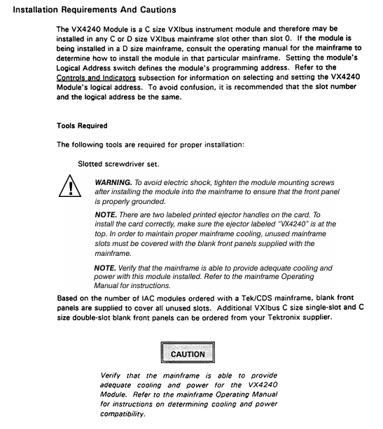
Installation and Operation Guide
1. Preparation and requirements before installation
(1) Tools and Environment
Essential tool: Phillips screwdriver.
Environmental requirements: The mainframe should provide sufficient heat dissipation (2.7 liters/second airflow, pressure drop of 0.19 mm H ₂ O, module temperature rise<10 ° C), operating temperature of 0 ° C~55 ° C, storage temperature of -40 ° C~85 ° C, relative humidity<75% (non condensing, 31 ° C~40 ° C).
(2) Switch settings (critical configuration, incorrect settings will cause module failure)
Description of switch name and position requirements
Logical address switch (S080) 1-255 (FFh is dynamically configured) base address calculation formula: [(64d × XYh)+49152d], it is recommended to match the slot number
The interrupt level switch (S081) 1-7 (0/8/9 disable interrupts) needs to match the interrupt handling level of the system controller
The Halt switch (S084) must be set to ON, otherwise the module cannot respond to VXIbus resource manager commands properly
The Bootstrap switch (S56) is set to OFF for factory testing purposes, and users do not need to adjust it
The memory size switch (S083) is preset by the factory and cannot be adjusted by oneself. It matches the hardware configuration of the memory
(3) Installation steps
Record the revised version of the module, serial number (top shield label), and switch settings, and fill in the installation checklist.
Confirm that the power supply of the host rack is turned off, and insert the module into any C/D size slot except for slot 0 (the D-size host rack should be adapted according to the host rack manual).
Tighten the module fixing screws to ensure that the front panel is grounded and avoid the risk of electric shock.
Connecting cables: The BNC interface uses RG58 coaxial cable to connect the device under test (UUT), while the DB25 interface can use CDS 73A-742P shielded connectors.
Check the overhead idle slot of the host: it needs to be covered with a blank panel to ensure heat dissipation; If there is a vacant slot on the left side of the module, the VME daisy chain jumper needs to be installed according to the host rack manual.
2. Basic operating procedures
(1) Parameter configuration (core command example)
Example Explanation of Operation Purpose Command
Set the sampling frequency F1E6 to 1 MHz (internal clock)
Configure input parameters VD5MF DC coupling, ± 5 V range, 50 Ω input impedance, differential input
Set the collection mode CR1000/50 recording mode, with 1000 samples per record and a total of 50 records
Configure trigger mode MP5.0 positive voltage threshold trigger (5.0 V)
Set the trigger delay D200E-9 to start sampling with a delay of 200 ns after triggering
(2) Sampling and analysis process
Sending configuration commands: Send parameter configuration command strings (up to 160 bytes in length, using<LF>or; Separate multiple commands.
Start sampling: Send the T (Trigger) command, the module enters the "standby" state (ARM LED lights up), and starts sampling after the triggering conditions are met (MIP LED lights up).
Data storage: Sampling data is stored in memory according to the set mode, and is automatically triggered again in recording mode until the set number of records is completed.
Signal analysis: Send A-series commands (such as AA calculating mean, AC executing FFT), and the module returns the analysis results.
Status query and error handling:
Send Q command to query module status (self-test results, sampling progress, trigger status, etc.).
Send the E command to read the error code (such as 02 indicating CPU memory failure, 08 indicating threshold out of range). The operation can only continue after the error code is cleared.
(3) Data output
Output format: Supports ASCII, binary, complement binary, ASCII block transmission (K option, block size 1-2500).
Address control: Supports automatic address increment/decrement, and can specify the offset address relative to the trigger point (- RAMsize to+RAMsize).
Step size setting: Optional 1-65536 sampling point step size, supports interval reading of data (such as reading 1 sample every 4 samples, suitable for multiplexing scenarios).
3. Self inspection and calibration
(1) Self checking function
Power on self-test: The module is completed within 5 seconds after power on, detecting core components such as CPU memory, A/D converter, and analog front-end. If it passes, the POWER LED will remain on and the SYSFAIL LED will turn off.
Command self-test: Send the S command to initiate an extended self-test (detecting all memory, calibration parameters, trigger circuits, etc.), and return to the default power on state after completion. The results can be obtained through the Q command (querying self-test status) or the E command (reading fault error codes).
(2) Calibration requirements and operations
Calibration cycle: It is recommended to calibrate every 12 months at operating temperature, and the module should be preheated for 10 minutes before calibration.
Calibration command:
KS [range]: Simultaneously calibrate the gain and offset within a specified voltage range (results stored in non-volatile memory).
KG [range]: Only calibrate the gain.
KO [range]: Only calibrate offset.
K [range]: Software calibration, returns offset voltage (not stored, used to compensate for temperature drift).
Calibration conditions: High precision DC calibration source (accuracy 0.1%), function generator (1 MHz, accuracy 0.002%) and other equipment should be used, operated by professional personnel.
Maintenance and troubleshooting
1. Daily maintenance
Cleaning: Regularly wipe the surface of the module with a dust-free cloth to remove dust; Stubborn stains can be wiped with diluted cleaning agents, and the use of abrasive cleaning agents is prohibited.
Fuse replacement: The module is equipped with+5V, -2V, ± 24V fuses (+5V uses Littelfuse 273005 2A fast melting type, others use 273002 2A fast melting type). After the fuse is blown, the fault needs to be eliminated before replacement.
Spare parts procurement: Ordering spare parts through Tektronix local offices or distributors requires providing product model, serial number, and revised version.
2. Common troubleshooting
Troubleshooting steps for possible causes of fault phenomena
SYSFAIL LED is always on. 1. Power failure (+5V/-2V/± 24V loss); 2. Self inspection failed; 3. CPU malfunction: 1. Check if the POWER LED is turned off. If it is off, replace the fuse; 2. Send the S command to perform extended self-test, and send the E command to read error codes; 3. Contact technical support for maintenance
No sampling data (MIP LED not lit) 1. Trigger condition not met; 2. Sampling frequency/period setting error; 3. Insufficient memory 1. Check trigger mode and threshold settings (M command); 2. Verify the sampling frequency command (F/P command); 3. Reduce the sample size of a single record or expand memory
Large deviation in analysis results: 1. uncalibrated or expired calibration; 2. Incorrect input parameter settings (range, coupling, impedance); 3. Insufficient sampling frequency (not satisfying Nyquist theorem) 1. Execute KS command to calibrate the corresponding voltage range; 2. Verify the parameters of the V command (ensure they match the signal); 3. Increase the sampling frequency (at least twice the highest frequency of the signal, recommended to be more than 10 times)
Communication failure: 1. Logical address setting conflict; 2. VXIbus bus failure; 3. Command format error: 1. Reset the logical address (to avoid conflicts with other modules); 2. Check the bus connection of the host rack; 3. Ensure that the command string conforms to syntax (ASCII characters, correct delimiter)
Extension options and compatibility
1. Extension options
Option 01:512K word sampling memory expansion.
Option 02: 1M word sampling memory expansion.
Option 2A (waveform output): Supports digital signal playback, programmable delay (200 ns to 420 s), output amplitude ± 1Vpp or ± 10Vpp (50 Ω load), and needs to be used in conjunction with a waveform output card.
2. Compatibility
Host rack compatibility: Supports all C/D size host racks that comply with VXIbus specifications, and Slot 0 requires a resource manager (such as VX4521).
Interface compatibility: Supports VXIbus serial protocol, compatible with IEEE-488 (GPIB) interface (requires conversion through Slot 0 module), configurable interrupt level (1-7 levels).
Software compatibility: Provides BASIC programming language sample programs and supports mainstream measurement and control software (must follow VXIbus instrument protocol commands).
Summary of Key Appendix Information
1. Appendix Core Content
Appendix A (VXIbus Operations): Detailed explanation of module VXIbus register definition, transfer mode (normal transfer/fast handshake), and interrupt handling process.
Appendix B (I/O Connections): Provide pin definitions, signal grounding requirements, and external trigger/clock/ARM signal interface specifications for BNC and DB25 connectors.
Appendix E (Fourier Transform): Explain the FFT principle, spectral leakage suppression (window function effect), and sampling frequency selection principle (Nyquist theorem).
Appendix H (Performance Verification): Provide the verification process and equipment requirements for key indicators such as DC accuracy, AC accuracy, and Common Mode Rejection Ratio (CMRR).
Appendix I (Calibration Process): Detailed description of the operation steps and adjustment of potentiometer positions for DC gain/offset calibration, AC gain calibration, and common mode rejection calibration.
2. Important Notice
Binary transmission: When using the National Instruments GPIB-VXI/C Slot 0 module, a dedicated code instrument (CI) needs to be loaded to avoid data buffer residue.
IEEE-488 address configuration: If the GPIB address is not assigned after the system is powered on, the Slot 0 resource manager delay (set to 5 seconds) needs to be adjusted to ensure that the module completes self-test.
- YOKOGAWA
- Reliance
- ADVANCED
- SEW
- ProSoft
- WATLOW
- Kongsberg
- FANUC
- VSD
- DCS
- PLC
- man-machine
- Covid-19
- Energy and Gender
- Energy Access
- Renewable Integration
- Energy Subsidies
- Energy and Water
- Net zero emission
- Energy Security
- Critical Minerals
- A-B
- petroleum
- Mine scale
- Sewage treatment
- cement
- architecture
- Industrial information
- New energy
- Automobile market
- electricity
- Construction site
- HIMA
- ABB
- Rockwell
- Schneider Modicon
- Siemens
- xYCOM
- Yaskawa
- Woodward
- BOSCH Rexroth
- MOOG
- General Electric
- American NI
- Rolls-Royce
- CTI
- Honeywell
- EMERSON
- MAN
- GE
- TRICONEX
- Control Wave
- ALSTOM
- AMAT
- STUDER
- KONGSBERG
- MOTOROLA
- DANAHER MOTION
- Bentley
- Galil
- EATON
- MOLEX
- Triconex
- DEIF
- B&W
- ZYGO
- Aerotech
- DANFOSS
- KOLLMORGEN
- Beijer
- Endress+Hauser
- schneider
- Foxboro
- KB
- REXROTH
- YAMAHA
- Johnson
- Westinghouse
- WAGO
- TOSHIBA
- TEKTRONIX
- BENDER
- BMCM
- SMC
- HITACHI
- HIRSCHMANN
- XP POWER
- Baldor
- Meggitt
- SHINKAWA
- Other Brands
- UniOP
- KUKA
- IBA
- Beckhoff
-
ADLINK CPCI-6860A - 51-31310-OB10 industrial motherboard CompactPCI SBC
-
ADLINK AmITX-SL-G-H110 - 51-7A104-0A30 Mini-ITX Industrial Motherboard
-
ADLINK PXI-2005-003 - CPCI Industrial PC Data Acquisition Card Multi-Function DAQ
-
ADLINK DININ-814M - 51-14032-0A3D SCSI-100P cable connection Interface Terminal Board
-
ADLINK CPCI-3920NA/C2D15/M1G - 3U CompactPCI Intel Core 2 Duo Single Board Computer
-
ADLINK PCIE-8560 - 51-18014-0A20 Communication Card High Speed DAQ
-
ADLINK PCI-C154+ - Motion Control Card 4-axis Motion Controller Board
-
ADLINK PCI-RTV24 - image capture card Analog Video Frame Grabber
-
ADLINK NuPRO-842LV/P - 51-41360-0B30 Industrial Motherboard CPU Board
-
ADLINK cBP-3208/3208R - CPCI Board 3U 8-Slot CompactPCI Backplane
-
ADLINK PCI-8164 - 4-Axis Motion Controller PCI Card 51-12406-0A40
-
ADLINK PCIe-GIE64+ - 4-CH GigE Vision PoE+ Frame Grabber Video Capture Card
-
ADLINK CPCI-6860 / 6860A - CompactPCI Dual Xeon Single Board Computer
-
ADLINK IEC-915GV - REV 1.1 Industrial motherboard CPU Board
-
ADLINK ND-6520 - Technology RS-232 to RS-422RS-485 Converter NuDAM Module
-
ADLINK RTV-24 / PCI-MP4S - 51-12519-1C30 4-Channel Real Time Video Capture Board
-
ADLINK cPCI-6910 / cPCI-6910AM/M1G - cPCI-6910AM/DXL16/M1G/S80G(G)-3120 BOARD CompactPCI SBC
-
ADLINK NUPRO-A40H - Linghua 51-41807-1A30 Industrial Control Computer Motherboard
-
ADLINK USB-3488A - USB to GPIB INTERFACE USB-3488A(G) Controller Module
-
ADLINK PCI-8134A - motion control card 4-Axis Controller Card
-
ADLINK PCI-7432 - Board 32-Channel input / 32-output Isolated Digital I/O PCI Card
-
ADLINK PCI-8134A - 51-12421-0A10 motion controller card tested
-
ADLINK LPCIe-7230 - 32 CH Isolated Input/output Card 2 Interrupts Low Profile PCIe
-
ADLINK NuPRO-E340 - industrial computer motherboard 51-47807-0A30 PICMG 1.3 SHB
-
ADLINK PCI-7434 - High-speed Digital Acquisition Card 64-CH Isolated DO Card
-
ADLINK NuPRO-E330 - 51-41805-0A20 Indsutrial Board SHB Single Board Computer
-
ADLINK PCI-7248 - OPTO-22 48 CHANNEL DIO DIGITAL TTL/DTL I/O 51-12006-0A40 GP
-
ADLINK PCI-8134 - Motion control card 4-Axis Controller Card
-
ADLINK AMP-208C - Movimiento Control Tarjeta 51-12420-1A20 W/Expansión & Breakout
-
ADLINK PCI-8164 - 51-12406-0A40 PCB Board 4-Axis Motion Controller Card
-
ADLINK DIN-68Y-SGII / DIN-68M-J3A - Terminal Board Connector Interface Block
-
ADLINK PCIe-7432 - Technology 51-18402-0A10 PCIe Card With High Input Range
-
ADLINK PCI-8144 / PCI-8144N - Motion control card 4-Axis Stepper Controller Card
-
ADLINK HSL-HUB3/REPEATER - HIGH SPEED LINK EXTENSION MODULES Distributed Hub Module
-
ADLINK ND-6017 - Data Logging + Acquisition 8CH A/D input Mod NuDAM Module
-
ADLINK LPCIe-7250 - data acquisition card Low Profile 8-CH Relay Output Card
-
ADLINK PCI-7432 - I/O card 64-CH Isolated Digital Input Output PCI Card
-
ADLINK IMB-M43H - industrial control computer motherboard Q87 Chip Micro-ATX
-
ADLINK MP-C154 - Motion control Card 4-Axis Motion Controller Board
-
ADLINK PCI-RTV24 - image capture card Video Frame Grabber Card
-
ADLINK PCI-7250 - 8-CH Relay Output & 8-CH Isolated DI Card
-
ADLINK PCI-6308V - 8-CH 12-Bit Isolated Analog Output PCI Card PCB-I-E-1148=6EX2
-
ADLINK PCI-7248 - capture card 48-CH Opto-22 Compatible DIO Card
-
ADLINK HSL-AI16A02-M-VV - Analog Input Output Distributed Module
-
ADLINK NuPRO-A301 - Rev:1.4 NUPRO-A301 PICMG Full-Size Single Board Computer
-
ADLINK PCI-6208V-GL - 8-CH Voltage Analog Output PCI Card
-
ADLINK PCI-8134A - 51-12421-0A10 4-Axis Motion Controller Card
-
ADLINK MNET-S23 - TECHNOLOGY MNET S23 - SERVO DRIVER CONTROL MODULE
-
ADLINK M-342 - ATX I3 I5 I7 Q67 Industrial Motherboard
-
ADLINK NUPRO-780 - Industrial Motherboard CPU Board PICMG SBC
-
ADLINK MP-C154 / MP-C152 - 4-Axis Motion Control Card Pulse-Train Controller
-
ADLINK NuPRO-935A/LV10B0 - Motherboard 51-41802-0A10 GP w/RAM Industrial Control Board
-
ADLINK MP-C154 - Motion control card 4-Axis Motion Controller Mainboard
-
ADLINK PCI-7250 - PCI Acquisition Card 8-CH Relay Output Isolated DI Card
-
ADLINK ACL-7124 - Technology Inc.24 DIO Card Digital Input Output Card
-
ADLINK PCI-8554 A2 - Timer/Counter Data Acquisition Card
-
ADLINK DIN-825-GP4 - Terminal Block Interface Board Breakout Module
-
ADLINK NuPR0-761 - REV:1.1 Industrial motherboard Full-Size PICMG SBC
-
ADLINK MXE-1401/M8G (G) - Matrix Fanless Embedded Computer Industrial PC
-
ADLINK HSL-DI16DO16-UD-NN - Digital 16 Channel I/O Mod Distributed I/O Module
-
ADLINK ND6520 - NUDAM INTELLIGENT DA&C MODULE RS232-RS-422/RS485 CONVERTOR
-
ADLINK NUPRO-761 - REV:1.1 Industrial Motherboard CPU Board
-
ADLINK AMP-208C - Motion Control Card 51-12420-1A20 DSP-based 8-axis
-
ADLINK NuPRO-A301REV 1.4 - with packaging industrial computer motherboard PICMG SBC
-
ADLINK PCM-9112+ - 51-12300-0A2 industrial motherboard Multi-Function DAQ PC/104 Module
-
ADLINK PCM-7250+ - 8-CH Relay Outputs & 8-CH Isolated DI Module PC/104
-
ADLINK PCI-RTV24 - Image capture card Analog Video Frame Grabber
-
ADLINK PCI-8134 - Motion Controller PCI Card 4-Axis Controller Board
-
ADLINK PCI-7432 - Isolated Digital I/O PCI Card
-
ADLINK PCI-8554 A2 - acquisition card Timer/Counter Card
-
ADLINK PCI-8132 - Rev.A2 2-Axis Servo & Stepper Motion Controller Card
-
ADLINK PCI-8132 - Data Acquisition card 2-Axis Motion Controller Card
-
ADLINK EBP-13E4 - 51-46703-0A30 Industrial Backplane Board Passive Backplane
-
ADLINK PCI-800L - Electronic Card Interface Controller Card
-
ADLINK PCIe-GIE72 - 51-18531-0A10 PCB Board GigE Vision Frame Grabber
-
ADLINK DAQ-2010(G)-OOBO - Simultaneous-Sampling Multi-Function DAQ Card
-
ADLINK PCI-9112 - REV.B1 Multifunction DAQ Card Data Acquisition Card
-
ADLINK PCI-7230 - 51-12003-DA60 32-CH Isolated Digital I/O Card
-
ADLINK PCI-7432 - Data Acquisition Card Isolated Digital I/O PCI Card
-
ADLINK ETX-AT-N270-18/LXE - 51-71111-0A20 ETX CPU Module Motherboard
-
ADLINK HSL-DI32-UD-N - DIGITAL INPUT 32 POINTS MODULE Distributed I/O
-
ADLINK AMP-204C - Motion Control card DSP-Based 4-Axis Advanced Controller
-
ADLINK MNET-4XMOG-0050 - Four-axis Motion Controller Distributed Motion Module
-
ADLINK AMP-204C - Motion control card DSP-Based 4-Axis Pulse-Train Controller
-
ADLINK PCI-7442 - Switch card 64-Channel Datalogging & Acquisition Card
-
ADLINK M-302 - Industrial control motherboard ATX PC Board
-
ADLINK NUPRO-852 / NUPRO-852LV - Industrial motherboard Single Board Computer
-
ADLINK PCI-8134 - REV.B1. 4-Axis Motion Controller Card
-
ADLINK PCI-GIE62 + - 51-18502-0A20 2-CH GigE Vision Frame Grabber PoE Card
-
ADLINK PCI-MPG24 - 51-12523-0B20 MPEG4 Card Video Compression Hardware
-
ADLINK HSL-TB32-M-DIN - 32-CH I/O TERMINAL W/ HSL-AI16AO2-M-VV MODULE
-
ADLINK PCI-M114-GL - PCB Ver 2.1 Motion Controller Axis Card
-
ADLINK IMB-M40H - SYM76996H61 motherboard Industrial Computer Mainboard
-
ADLINK NUPRO-A40H - 51-41807-1A20 industrial control motherboard H61 Chip
-
ADLINK PCI-M114-GL - Axis Card Data Acquisition Card PCB VER2.2 Motion Controller
-
ADLINK PCI-8134 - Motion Controller PCI Card 4-Axis Controller Board
-
ADLINK PCI-8102 - Motion control card 2-Axis Servo & Stepper Controller
-
ADLINK NuPRO-841REV:3.0 - motherboard Industrial Control PC Board
-
ADLINK HSL-TB32-U-DIN REV A1 - Breakout Terminal Board Field I/O Module
-
ADLINK AMP-204C - Motion Control card DSP-Based 4-Axis Pulse-Train Controller
-
ADLINK NUPRO-A40H - 51-41807-1A20 industrial control motherboard H61 PC Board
-
ADLINK PCI-6308A / PCI-6308V - 51-12202-0A50 Isolated Analog Output Card
-
ADLINK AMP-204C - DSP-Based 4-Axis Advanced Pulse-Train Motion Controller
-
ADLINK PCI-7434 - Technology 64-Channel Isolated Digital I/O PCI Cards
-
ADLINK CPCI-6840 / CPCI-6840V / PM16/M1G-12G0 - CompactPCI Single Board Computer CPU Module
-
ADLINK PCIE-GIE74 - Motherboard Video Capture Card 51-18531-0A10 Frame Grabber
-
ADLINK NuPRO-E330 - industrial computer equipment motherboard Control Mainboard
-
ADLINK AMP-208C / 51-12420-1A20 - Motion Control Card W/ Expansion & Breakout Board
-
ADLINK HPCI-14S12U - industrial computer baseboard Passive Backplane 14 Slots
-
ADLINK PCI-8164 - 4-Axis Motion Controller PCI Card W/ 1x Cable, 1x Breakout Box
-
ADLINK PCIe-RTV24 - 51-18016-0A20 Image Acquisition Video Capture Card
-
ADLINK M-342 - 5 PCI ATX Motherboard Industrial PC Mainboard
-
ADLINK PCI-FIW64 - 4/2 Channel IEEE1394B Image Capture Card FireWire Frame Grabber
-
ADLINK PCI-7432 - digital IO card 64-CH Isolated Digital Input Output Card
-
ADLINK 51-12001-0C20 - Circuit Board PCI-7200 Data Acquisition Controller Card
-
ADLINK PXI-3920 - PXI 3U cPCI Industrial Controller Embedded System CPU Board
-
ADLINK NuPRO-841REV:2.0 - motherboard Industrial Control PC Board
-
ADLINK NuPro-E330 - 51-41805-0A20 PCB Industrial Control Computer Motherboard
-
ADLINK PCI-RTV24 - Image capture card Analog Video Frame Grabber
-
ADLINK PCI-7442 - Switch card 64-Channel Datalogging & Acquisition Card
-
ADLINK HPX-13S4 - device baseboard Passive Backplane Riser Card
-
ADLINK PCI-9112 REV A.1 - Multi Function DA&C Board Data Acquisition Card
-
ADLINK PCI-7248 - 51-12006-0A40 Card Control 48-CH Digital I/O Module
-
ADLINK CPCI-6860 / 6860A - motherboard CompactPCI Dual Xeon Single Board Computer
-
ADLINK DPAC-3020-11(G) - Embedded PC Automation Controller Machine Control Board
-
ADLINK NuPRO-841 REV:1.0 - industrial control motherboard CPU Board
-
ADLINK MNET-4XMOG-0050 - Four-axis Motion Controller MNET Motion Control Card
-
ADLINK ETX-AT-N270-18/LXE - 51-71111-0A20 ETX CPU Module Motherboard

K-JIANG

Add: Jimei North Road, Jimei District, Xiamen, Fujian, China
Tell:+86-15305925923